Nanosecond digital programmable delay circuit based on FPGA (Field-Programmable Gate Array)

A delay circuit, nanosecond technology, applied in program control, instrument, computer control, etc., can solve the problems of large delay time scale, poor delay accuracy, fixed delay time, etc. High applicability and versatility, controllable delay time effect

Active Publication Date: 2015-07-01
无锡长元新能源电动车科技发展有限公司
View PDF1 Cites 0 Cited by
  • Summary
  • Abstract
  • Description
  • Claims
  • Application Information

AI Technical Summary

Problems solved by technology

[0003] The current delay circuit is mainly divided into analog delay circuit and digital delay circuit. The analog delay circuit has the disadvantages of large delay time scale, fixed delay time and poor delay accuracy due to the use of analog devices to generate delay. limit its application
The digital delay circuit has the advantages of high delay precision and programmable time, but it can only be realized by a dedicated chip at present. However, the dedicated programmable delay chip is generally more expensive and has more pins, which brings great difficulties to the circuit design. great inconvenience

Method used


Image

  • Nanosecond digital programmable delay circuit based on FPGA (Field-Programmable Gate Array)
  • Nanosecond digital programmable delay circuit based on FPGA (Field-Programmable Gate Array)
  • Nanosecond digital programmable delay circuit based on FPGA (Field-Programmable Gate Array)

Examples


Embodiment Construction

[0015] In order to make the object, technical solution and advantages of the present invention clearer, the present invention will be further described in detail below with reference to the accompanying drawings.

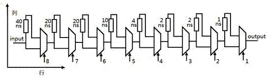
[0016] The FPGA-based nanosecond-level digital programmable delay circuit of the present invention is formed by cascading programmable delay units; the programmable delay unit is composed of a two-to-one selector and a vertical delay unit, and the specific structure is as follows figure 1 shown. figure 1 The delay circuit shown can realize any delay of 0~99ns; according to the needs of users, the delay circuit can be expanded to realize any time delay circuit. The present invention uses figure 1 The circuit shown is taken as an example to illustrate the specific implementation of the invention. The delay generated by the signal passing through the one-two selector in the programmable delay unit structure is the system delay of the circuit of the present invention. ...


PUM


Abstract

The invention discloses a nanosecond digital programmable delay circuit based on an FPGA (Field-Programmable Gate Array). The delay circuit is composed of a programmable transverse selector and a longitudinal delay unit capable of realizing different delay time. The transverse selector is formed by a plurality of either-or selectors in cascade connection; the longitudinal delay unit is formed by different numbers of basic delay units in cascade connection; the transverse selector realizes programmable delay through controlling input signals to pass through the longitudinal delay unit or not, and realizes precise and controllable delay by a locating and wiring restriction technology. The nanosecond digital programmable delay circuit disclosed by the invention can realize precise nanosecond delay by the programming and by the FPGA design, the precision is high, the versatility and the applicability are strong.

Description

technical field [0001] The invention belongs to a delay circuit, in particular to a nanosecond-level digital programmable delay circuit based on FPGA. Background technique [0002] Because the delay circuit can delay the input signal, it is widely used in clock phase modulation, parallel signal timing calibration and target echo simulation. The delay circuit can adjust the phase of the clock, so that the clock signal and the sampled signal meet the sampling phase relationship, and can also adjust the parallel signal to calibrate the phase deviation in the parallel signal transmission process. In the target echo simulator, the delay circuit can be applied to simulate the continuous echo of moving targets. [0003] The current delay circuit is mainly divided into analog delay circuit and digital delay circuit. The analog delay circuit has the disadvantages of large delay time scale, fixed delay time and poor delay accuracy due to the use of analog devices to generate delay. ...

Claims


Application Information

Patent Timeline
Patent Type & Authority Patents(China)
IPC IPC(8): G05B19/042
Inventor 李洪涛朱晓华顾陈曾文浩
Owner 无锡长元新能源电动车科技发展有限公司
Why Eureka
Try Eureka