
Time Delay Device Based on Tunneling-Induced Transparency Effect of Quantum Well Subband Transition

A technology for inducing transparent and deep quantum wells, applied in instruments, nonlinear optics, optics, etc., can solve problems such as short delay time and high interaction intensity, and achieve long delay time and controllable delay time

Active Publication Date: 2016-03-30
JILIN UNIV
View PDF5 Cites 0 Cited by
  • Summary
  • Abstract
  • Description
  • Claims
  • Application Information

AI Technical Summary

Problems solved by technology

Compared with the coupling interaction of the microcavity structure itself using semiconductor superlattice materials, the atomic system has disadvantages such as excessive interaction strength, short delay time, and inability to work at the wavelength of communication.

Method used


Image

  • Time Delay Device Based on Tunneling-Induced Transparency Effect of Quantum Well Subband Transition
  • Time Delay Device Based on Tunneling-Induced Transparency Effect of Quantum Well Subband Transition

Examples


Embodiment 1

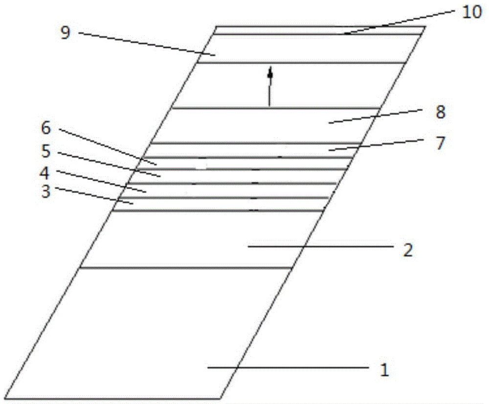
[0022] refer to figure 1 , substrate 1 is GaAs (001). Followed by the AlAs layer, the thickness is 3900nm; the first barrier layer 3, the composition is Al 0.4 Ga 0.6 As, the thickness is 20nm; the shallow quantum well layer 4, the composition is Al 0.16 Ga 0.84 As, the thickness is 6.7nm; the second barrier layer 5, the composition is Al 0.4 Ga 0.6 As, the thickness is 4.2nm; the deep quantum well layer 6 is composed of GaAs, and the thickness is 7.8nm; the third barrier layer 7 is composed of Al 0.4 Ga 0.6 As, the thickness is 2.9nm; the continuum 8, the composition is Al 0.16 Ga 0.84 As, the thickness is 160nm. From the first barrier layer 3 to the continuous region 8 is a cycle, and then grow 9 cycles, a total of 10 cycles, and then grow a cover layer 9, the composition is Al 0.4 Ga 0.6 As, with a width of 200nm, and a GaAs air spacer layer 10, with a width of 7.5nm. The working wavelength of the time delay device with this structure is 9.23 μm, and the time d...

Embodiment 2

[0024] refer to figure 1 , substrate 1 is GaAs (001). In turn is the AlAs layer, the thickness is 5000nm; the first barrier layer 3, the composition is Al 0.35 Ga 0.75 As, the thickness is 10nm; the shallow quantum well layer 4, the composition is Al 0.1 Ga 0.9 As, the thickness is 8nm; the composition of the second barrier layer 5 is Al 0.35 Ga 0.75 As, the thickness is 3nm; the deep quantum well layer 6 is GaAs, the thickness is 10nm; the composition of the third barrier layer 7 is Al 0.35 Ga 0.75 As, the thickness is 2nm; the continuum 8, the composition is Al 0.1 Ga 0.9 As, the thickness is 160nm. From the first barrier layer 3 to the continuous region 8 is a cycle, and then grow 14 cycles, a total of 15 cycles, and then grow a cover layer 9, the composition is Al 0.4 Ga 0.6 As, with a width of 300nm, and a GaAs air spacer layer 10, with a width of 5nm. The time delay device with this structure has a working wavelength of 13.16 μm and a time delay of 0.55 ps. ...

Embodiment 3

[0026] refer to figure 1 , substrate 1 is GaAs (001). In turn is the AlAs layer, the thickness is 2000nm; the first barrier layer 3, the composition is Al 0.4 Ga 0.6 As, the thickness is 30nm; the shallow quantum well layer 4 is Al 0.2 Ga 0.8 As material, the thickness is 1.8nm; the composition of the second barrier layer 5 is Al 0.4 Ga 0.6 As, the thickness is 5nm; the deep quantum well layer 6 is GaAs, the thickness is 5.3nm; the composition of the third barrier layer 7 is Al 0.4 Ga 0.6 As, the thickness is 4.5nm; the composition of the continuum 8 is Al 0.2 Ga 0.8 As, the thickness is 160nm. From the first barrier layer 3 to the continuous region 8 is a cycle, and then grow 5 cycles, a total of 6 cycles, and then grow a cover layer 9, the composition is Al 0.4 Ga 0.6 As, with a width of 500nm, and a GaAs air spacer layer 10, with a width of 10nm. The working wavelength of the time delay device with this structure is 5.86 μm, and the time delay is 0.18 ps.


PUM

PropertyMeasurementUnit
thicknessaaaaaaaaaa
thicknessaaaaaaaaaa
thicknessaaaaaaaaaa

Abstract

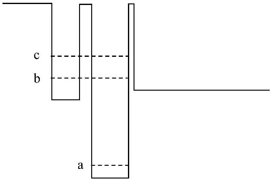
The invention belongs to the technical field of semiconductor materials, and relates to a time delay device based on the tunneling-induced transparency effect of quantum well sub-band transition, in particular to a time delay device used in the photoelectron field. The time delay device is structurally characterized in that an AlAs layer (2), a first barrier layer (3), a shallow quantum well layer (4), a second barrier layer (5), a deep quantum well layer (6), a third barrier layer (7) and a continuous area (8) grow on a substrate (1) of a GaAs material in sequence; six to fifteen cycles each of which is formed by a first barrier layer (3), a shallow quantum well layer (4), a second barrier layer (5), a deep quantum well layer (6), a third barrier layer (7) and a continuous area (8) are arranged; then, a covering layer (9) is arranged, and an air isolation layer (10) is arranged on the outermost layer. The delay time of the time delay device can reach the picosecond level, and the time delay device can be applied to the photoelectron field. The time delay device is more practical than a delay time device with an atom system, the structure and materials of the time delay device can be manually selected, and the coherent intensity of the time delay device can be controlled and changed.

Description

technical field [0001] The invention belongs to the technical field of semiconductor materials, in particular to a time delay device used in the field of optoelectronics. Background technique [0002] Optical time delay devices have application value in the field of optical information processing and processing, for example, encoding, decoding, filtering, and convolution calculation of optical signals. The existing similar optical time delay system is the atomic Lambda three-level system with electromagnetically induced transparency in the cavity. In the atomic three-level system, a beam of probe light and a beam of strongly coupled light are incident in parallel to the sample cell containing gas atoms, similar to the interaction between subbands |2> and |3> of the present invention This is achieved by strengthening the coherent field. Compared with the coupling interaction of the microcavity structure itself using semiconductor superlattice materials, the atomic sys...

Claims


Application Information

Patent Timeline
Patent Type & Authority Patents(China)
IPC IPC(8): G02F1/017
Inventor 苏雪梅王涛张锐李翠莉卓仲畅
Owner JILIN UNIV
Learn More