Semiconductor device and manufacturing method of the same

a technology of semiconductors and semiconductors, applied in the direction of pulse techniques, instruments, computations using denominational number representations, etc., can solve the problem of longer delay time, and achieve the effect of reducing development costs, reducing power consumption, and efficient delay circuits

Inactive Publication Date: 2006-02-16
RENESAS ELECTRONICS CORP
View PDF20 Cites 3 Cited by
  • Summary
  • Abstract
  • Description
  • Claims
  • Application Information

AI Technical Summary

Benefits of technology

[0019] It is possible to realize an efficient delay circuit, according to the universal logic cell, the semiconductor device using the same, and the manufacturing method of the semiconductor device of the present invention.
[0020] The development costs can be reduced, according to the

Problems solved by technology

In particular, the longer delay time is required as a clock

Method used


Image

  • Semiconductor device and manufacturing method of the same
  • Semiconductor device and manufacturing method of the same
  • Semiconductor device and manufacturing method of the same

Examples


first embodiment

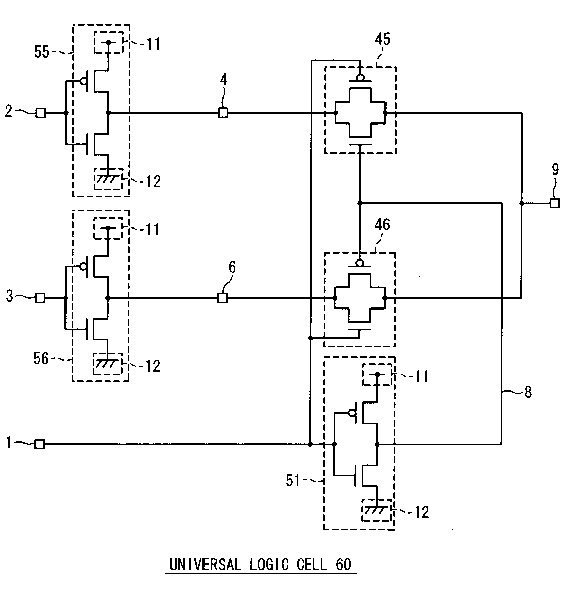
[0038]FIG. 1 is a circuit diagram showing a configuration of a universal logic cell 60 according to a first embodiment of the present invention. The universal logic cell 60 has a first inverter 55 and a second inverter 56 in a first stage, and a first transfer gate 45 and a second transfer gate 46 in a second stage. The first transfer gate 45 and the second transfer gate 46 are connected to an inverter 51. In other words, the universal logic cell 60 forms a two-input and output-inversion-type multiplexer (MUX).

[0039] The inverter 51 is an inverter of a general type, having a P-channel transistor connected to a power supply line 11 and an N-channel transistor connected to a ground line 12. Here, the power supply line 11 and the ground line 12 are interconnections to be used to apply power supply potential VDD and ground potential GND, respectively. An input and an output of the inverter 51 are connected to a node 1 and a node 8, respectively.

[0040] The first inverter 55 is also an ...

second embodiment

[0048]FIG. 4 is a circuit diagram showing a configuration of a universal logic cell 60′ according to a second embodiment of the present invention. The universal logic cell 60′ includes P-channel transistors 21 and 22, N-channel transistors 31 and 32, transfer gates 41 to 44, and an inverter 51.

[0049] The inverter 51 is an inverter of a general type, having a P-channel transistor connected to a power supply line 11 and an N-channel transistor connected to a ground line 12. Here, the power supply line 11 and the ground line 12 are interconnections to be used to apply the power supply potential VDD and the ground potential GND, respectively. An input and an output of the inverter 51 are connected to a node 1 and a node 8, respectively.

[0050] A gate, a source and a drain of the P-channel transistor 21 are connected to a node 2, the power supply line 11 and a node 4, respectively. Also, a gate, a source and a drain of the N-channel transistor 31 are connected to the node 2, the ground ...

third embodiment

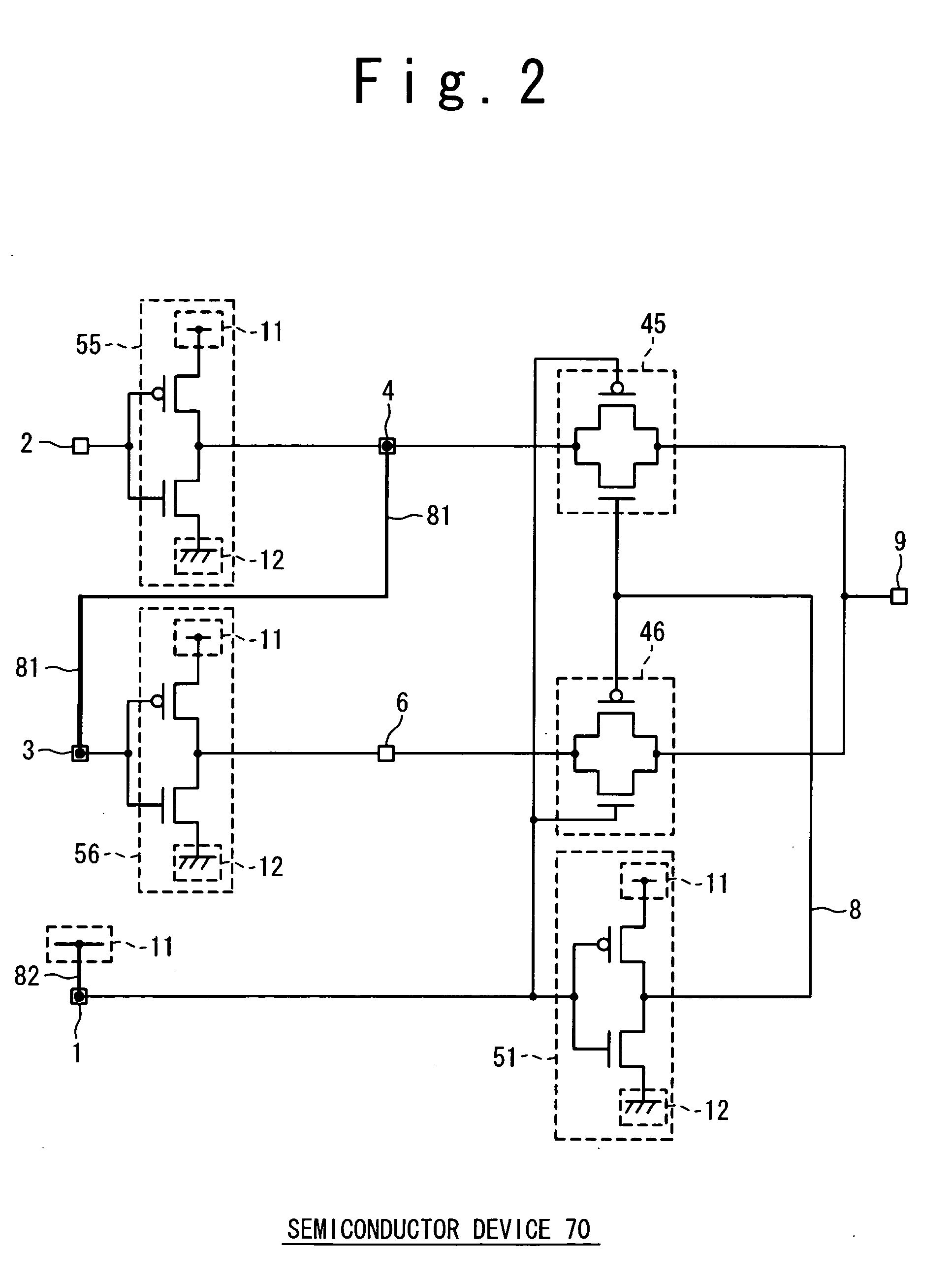
[0071] In a third embodiment of the present invention, the universal logic cell 60′ shown in FIGS. 4 to 7 is used as in the above-mentioned second embodiment. Therefore, description regarding the universal logic cell 60′ is omitted.

[0072]FIG. 9 is a circuit diagram showing a configuration of a semiconductor device 70B using the above-mentioned universal logic cell 60′ according to the present embodiment. The semiconductor device 70B shown in FIG. 9 has a first interconnection 81B and a second interconnection 82B in addition to the universal logic cell 60′ shown in FIG. 4. The first interconnection 81B and the second interconnection 82B are formed in the above-mentioned customize interconnection layers, and are connected with the exposed nodes and the ground line 12. More specifically, the first interconnection 81B connects the node 6, the node 7 and the node 2, while the second interconnection 82B connects the node 1 and the ground line 12. A method of manufacturing the semiconduct...


PUM


Abstract

A semiconductor device has a plurality of universal logic cells, a power supply line, a ground line, a first interconnection and a second interconnection. Each universal logic cell includes first to seventh nodes formed in a top layer of common interconnection layers which are allocated to the universal logic cells. The first interconnection connects the third node, the fourth node and the fifth node, and the second interconnection connects the power supply line and the first node. Or, the first interconnection connects the second node, the sixth node and the seventh node, and the second interconnection connects the ground line and the first node. The first and second interconnections are formed in a customize interconnection layer provided on the common interconnection layers.

Description

BACKGROUND OF THE INVENTION [0001] 1. Field of the Invention [0002] The present invention relates to a semiconductor device. More particularly, the present invention relates to a universal logic cell, a semiconductor device using the universal logic cell, and a method of manufacturing the semiconductor device. [0003] 2. Description of the Related Art [0004] A master slice method which is a semi-custom method is publicly known as one of conventional methods of developing a semiconductor device. As one type of the master slice method, a technique called “structured ASIC (Application Specific Integrated Circuit)” is proposed. [0005] According to the structured ASIC, for example, three lower layers of all six interconnection layers are commonly utilized as “common interconnection layers”, and the remaining three upper layers are provided as “customize interconnection layers”. In the common interconnection layers as the lower layers, such components as interconnections and nodes between ...

Claims


Application Information

Patent Timeline
IPC IPC(8): H03K19/173
CPCH03K19/20
Inventor YAMAMOTO, KENJI
Owner RENESAS ELECTRONICS CORP
Why Eureka
Try Eureka