Modeling method of etching yield in plasma etching process

A plasma and process technology, applied in the field of solving the etching yield model, can solve the problems of high measurement cost and good versatility

Inactive Publication Date: 2013-04-03
TSINGHUA UNIV
View PDF4 Cites 15 Cited by
  • Summary
  • Abstract
  • Description
  • Claims
  • Application Information

AI Technical Summary

Problems solved by technology

It can avoid the influence of the measuring instruments in the experiment on the etching rate or yield model, and solve the problem of high measurement cost; a

Method used


Image

  • Modeling method of etching yield in plasma etching process
  • Modeling method of etching yield in plasma etching process
  • Modeling method of etching yield in plasma etching process

Examples


Embodiment Construction

[0029] A modeling method of etching yield in a plasma etching process proposed by the present invention is described in detail in conjunction with the accompanying drawings and embodiments as follows:

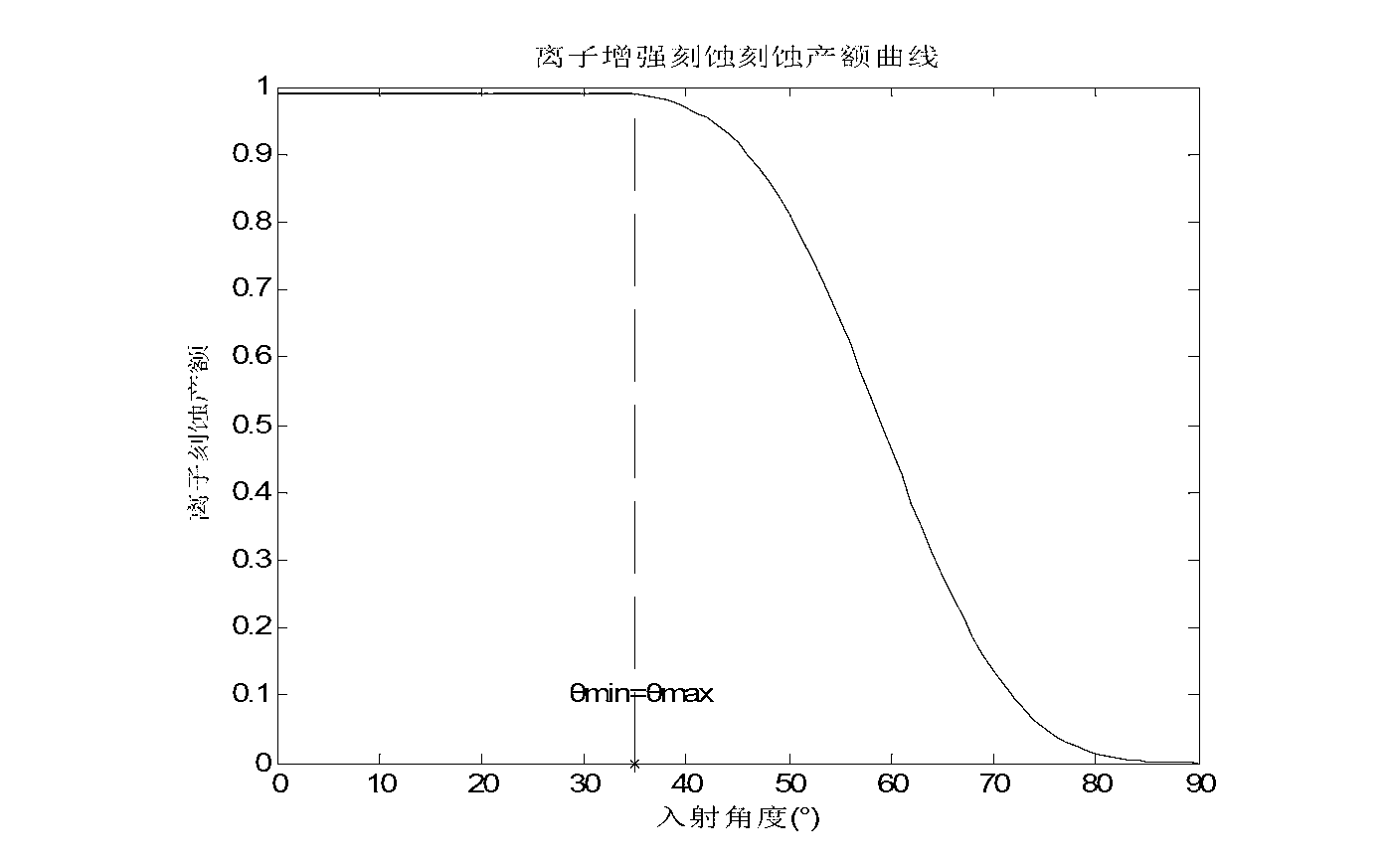
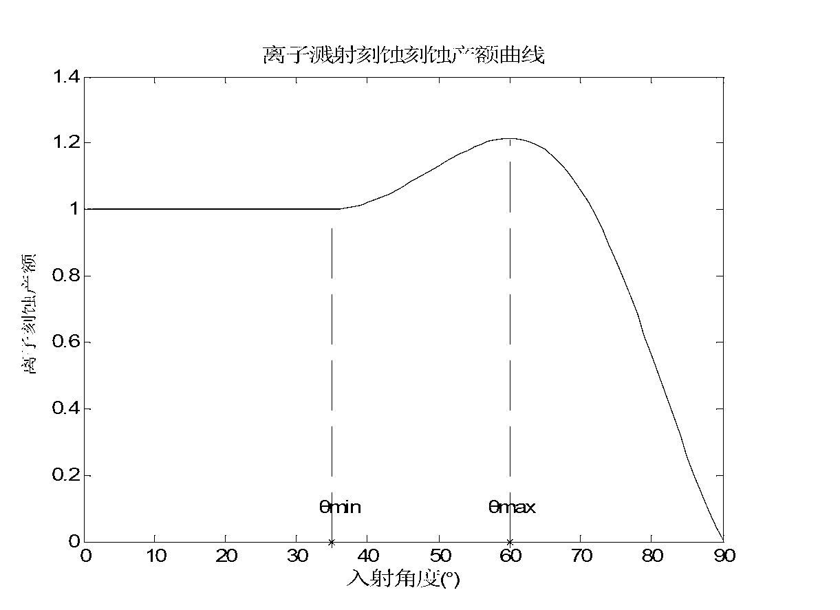
[0030] The overall process of the method embodiment of the present invention is as follows Figure 4 As shown, this embodiment proposes an etching yield model Y total The parameter means:

[0031]

[0032] The intermediate variables a and b in formula (1) are expressed as:

[0033] a = θ min tan ( θ max ) - θ max ...


PUM


Abstract

The invention relates to a modeling method of an etching yield in the plasma etching process, and belongs to the technical field of simulation of the etching process in the microelectronic processing procedure. The method comprises the following steps of: parametrically representing an etching yield model; adopting an optimization algorithm to obtain the optimal control parameters in the etching yield model by optimization; and in the optimization process, calculating the pros and cons of each group of control parameters (fitness value) by an etching profile evolution method to be used as a basis of selecting the optimization algorithm and generating the next-step control parameter set. The optimal model control parameter is substituted into a model parameterization formula to obtain the etching yield model. The impact of a measuring instrument on the model in an experiment can be avoided to solve the problem of high measuring cost; and meanwhile, the generality is good, and ditch grooves of different sizes are simulated at different etching times under the same process conditions by utilizing the model.

Description

technical field [0001] The invention belongs to the technical field of simulating the etching process in the process of microelectronics processing, and particularly relates to a method for solving an etching yield model by combining an optimization algorithm and an etching evolution method. Background technique [0002] With the development of microelectronics manufacturing technology, the size of a single component that constitutes an integrated circuit chip continues to shrink, while the area of ​​a single chip is getting larger and larger, resulting in higher integration of integrated circuits, making integrated circuits more complex and higher performance and a more economical direction. In this way, higher requirements are also put forward for microelectronics manufacturing technology. To break through the bottleneck of current manufacturing technology, people need a deep understanding of the basic mechanism of processing technology. Especially in the plasma etching p...

Claims


Application Information

Patent Timeline
IPC IPC(8): G06F17/50
Inventor 宋亦旭杨宏军孙晓民贾培发
Owner TSINGHUA UNIV
Why Eureka
Try Eureka