Electronic tag manufacturing method

A technology of electronic tags and manufacturing methods, which is applied in the field of radio frequency communication, can solve problems such as difficult use of metal surfaces, large size of electronic tags, and poor environmental adaptability of products, and achieve simple and easy manufacturing methods, convenient production, and good market competitiveness Effect

Inactive Publication Date: 2013-04-03
上海祯显电子科技有限公司
View PDF0 Cites 8 Cited by
  • Summary
  • Abstract
  • Description
  • Claims
  • Application Information

AI Technical Summary

Problems solved by technology

However, the conventional electronic label packaging process determines that the product has poor environmental adaptability, can no longer be used in harsh environments, cannot be impacted by external forces, is not easy to use on metal

Method used


Image

  • Electronic tag manufacturing method
  • Electronic tag manufacturing method

Examples


Embodiment Construction

[0032] In order to make the technical means, creative features, goals and effects achieved by the present invention easy to understand, the present invention will be further described below in conjunction with specific illustrations.

[0033] Adopting the manufacturing method of the electronic tag of the present invention can realize the industrialized production of small ultra-high frequency electronic tags, realize the miniaturization of the volume of ultra-high frequency electronic tags and products with high reliability, and then provide technical solutions and specific implementation methods as follows:

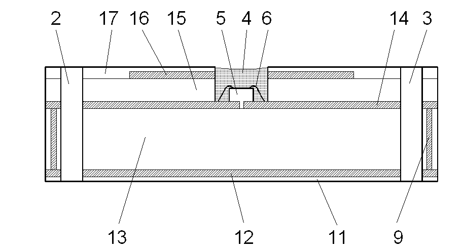
[0034] see figure 2 The cross-sectional schematic diagram of the electronic tag of the present invention, the antenna of the electronic tag is composed of the bottom solder resist layer 11, the ground plane metal layer 12, the antenna insulating medium layer 13, the signal radiation unit layer 14, the capacitor insulating medium layer 15, the capacitor The metal layer ...


PUM


Abstract

The invention discloses an electronic tag manufacturing method. The electronic tag manufacturing method includes the steps: (1) dispensing die attach adhesive in a chip mounting area of an electronic tag antenna; (2) mounting an electronic tag chip at the position dispensed with the die attach adhesive in the step (1); (3) performing high-temperature solidification for a semi-finished product obtained in the step (3), enabling the die attach adhesive to be solidified and then firmly fixing the chip on an antenna substrate; (4) carrying out lead bonding for a semi-finished product obtained in the step (3), and welding two pads on the chip and a pad of the electronic tag antenna together by the aid of an ultrasonic welding process; (5) carrying out an adhesive dispensing and filling process for a semi-finished produce obtained in the step (4), and filling epoxy resin filling adhesive into a chip mounting hole to enable the chip and a lead to be enveloped by the epoxy resin filling adhesive; (6) carrying out filling adhesive solidification for a semi-finished product obtained in the step (5), heating by infrared or ultraviolet and solidifying the epoxy resin filling adhesive; and (7) performing subsequent testing, personalizing, numbering and packaging processes for a finished product obtained in the step (6). An electronic tag manufactured by the method can have the advantages of small size, metal resistance and high reliability.

Description

technical field [0001] The invention relates to the field of radio frequency communication and the field of smart labels, in particular to a method for manufacturing an electronic label. Background technique [0002] In recent years, due to the continuous development of radio frequency electronic technology, especially the wide application of radio frequency electronic tags, people's way of life is gradually changing. Common radio frequency electronic tags are divided into two categories: active and passive in terms of power supply; in terms of carrier frequency, there are 125KHz (130KHz) low-frequency bands, 13.56MHz high-frequency bands, 433MHz, 915MHz ultra-high frequency bands , 2.4GHz, 5.8GHz microwave frequency band; the application of electronic tags is ubiquitous, so there are various shapes and products suitable for different application requirements, making people's life more convenient and efficient. [0003] In order to make radio frequency electronic tags more ...

Claims


Application Information

Patent Timeline
IPC IPC(8): G06K19/07
Inventor 陆红梅
Owner 上海祯显电子科技有限公司
Why Eureka
Try Eureka