
Shifting register, working method of shifting register, grid electrode driving device and display device

A shift register and gate connection technology, which is applied in the fields of shift registers, display devices, and gate drive devices, can solve problems such as improper opening of thin-film transistors, large circuit noise on gate lines, and circuit dysfunction, and achieve voltage elimination Effects of coupling noise, prolonging service life, and stabilizing operation

Active Publication Date: 2013-04-03
BOE TECH GRP CO LTD +1
View PDF5 Cites 23 Cited by
  • Summary
  • Abstract
  • Description
  • Claims
  • Application Information

AI Technical Summary

Problems solved by technology

[0004] However, it is well known that the clock signal is a square wave that periodically circulates between the first level and the second level, and includes a plurality of clock periods in one scan period when the scan signal circulates from the first row of pixels to the last row of pixels, and For a shift register, only half of the clock cycle is used to output the scan signal, and in other clock cycles that do not need to output the scan signal, the output end of the shift register is often also received by the clock signal The level of the output changes due to the influence of the gate line will cause a large circuit noise, which will cause the inappropriate turn-on of the thin film transistor in the pixel and make the circuit function disorder

Method used


Image

  • Shifting register, working method of shifting register, grid electrode driving device and display device
  • Shifting register, working method of shifting register, grid electrode driving device and display device
  • Shifting register, working method of shifting register, grid electrode driving device and display device

Examples


Embodiment Construction

[0032] The following will clearly and completely describe the technical solutions in the embodiments of the present invention with reference to the drawings in the embodiments of the present invention.

[0033] It should be clear that the described embodiments are only some of the embodiments of the present invention, not all of them.

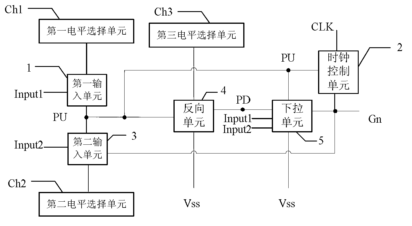
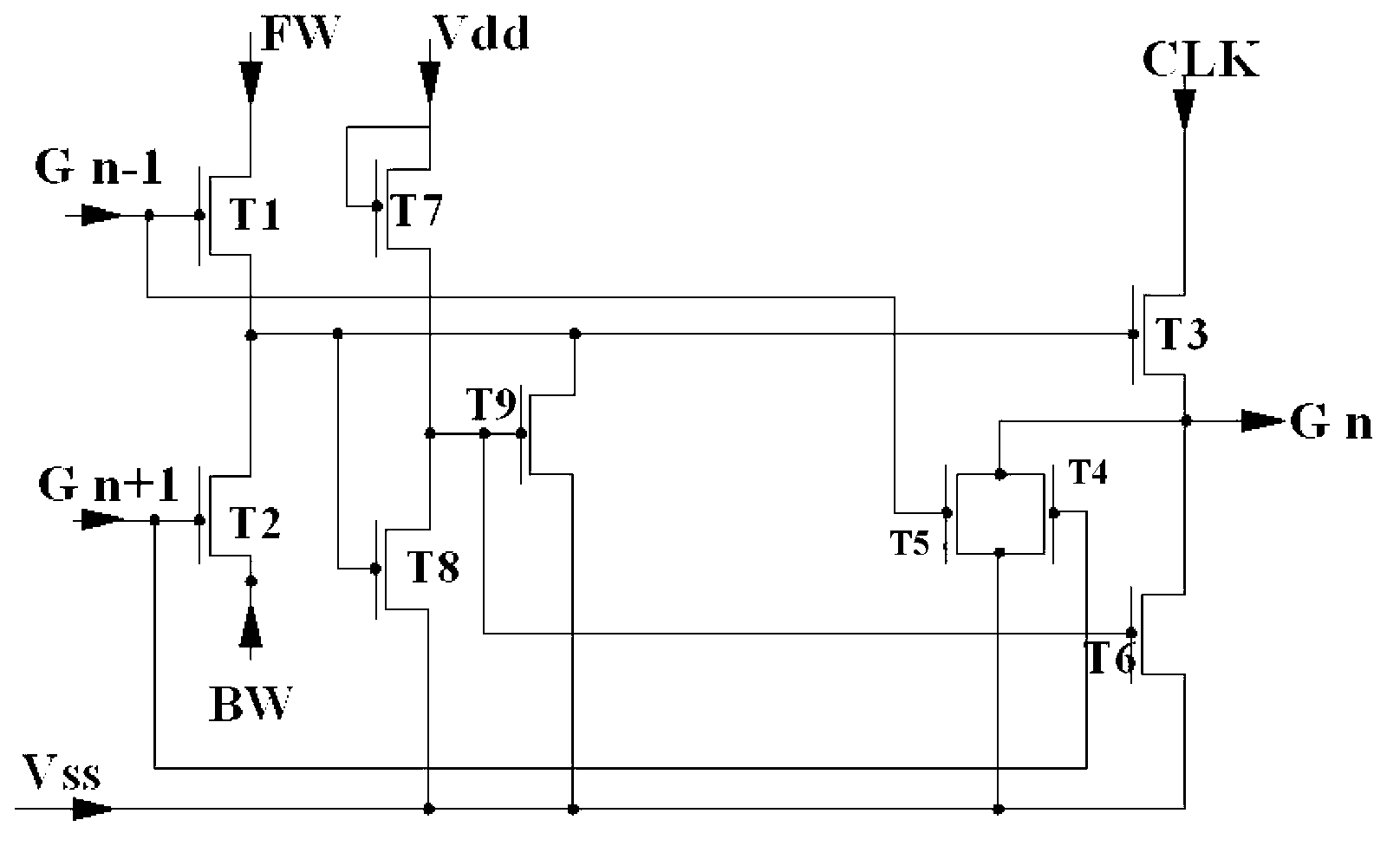
[0034] like figure 1 As shown, the embodiment of the present invention provides a shift register, including: a first input unit 1, a clock control unit 2, a second input unit 3, an inversion unit 4, a pull-down unit 5 and a first level selection unit Ch1 , the second level selection unit Ch2, and the third level selection unit Ch3.

[0035] The first input unit 1 is respectively connected to the first input signal Gn-1, the first level selection unit Ch1, and the second input unit 3, wherein the first input unit 1 and the second input The node connected to the unit 3 is a pull-up node PU, and the first input unit 1 is used to control the pote...


PUM


Abstract

The embodiment of the invention discloses a shifting register, a working method of the shifting register, a grid electrode driving device and a display device, relates to the technical field of displaying, and aims at effectively eliminating voltage coupling noise generated by clock signals at an output end of the shifting register. The shifting register comprises a first input unit, a clock control unit, a second input unit, a reverse unit, a pull-down unit, a first electrical level selection unit, a second electrical level selection unit and a third electrical level selection unit. The first input unit is respectively connected with a first input signal, a first electrical level selection unit and the second input unit, wherein a node where the first input unit and the second input unit are connected is a pull up node, and the first input unit is used for controlling electric potential of the pull up node. The shifting register, the working method of the shifting register, the grid electrode driving device and the display device can be used in various display devices.

Description

technical field [0001] The invention relates to the field of display technology, in particular to a shift register and a working method thereof, a gate driving device and a display device. Background technique [0002] Liquid crystal display products are widely used in various fields of production and life. When displaying, the liquid crystal display drives each pixel in the liquid crystal panel to display through a driving circuit. The driving circuit of the liquid crystal display mainly includes a gate driving circuit and a data driving circuit. Wherein, the data driving circuit is used for sequentially latching the input data and clock signal and converting the latched data into an analog signal and inputting it to the data line of the liquid crystal panel. The gate driving circuit is used to convert the clock signal into an on / off voltage through a shift register (Shift Register, SR), and output it to each gate line of the liquid crystal panel respectively. Wherein, on...

Claims


Application Information

Patent Timeline
IPC IPC(8): G09G3/20G09G3/36G11C19/28
CPCG09G3/3677G11C19/28G09G2320/0209G09G2310/0283G09G2310/08G09G2320/043G09G2310/0286G09G3/3688G09G3/3648G09G3/3611G11C19/20G09G2310/0264
Inventor 谷晓芳马睿胡明
Owner BOE TECH GRP CO LTD
Learn More