Method for forming semiconductor integrated device

A technology of integrated devices and semiconductors, which is applied in the field of semiconductor integrated device formation, can solve the problems of many process steps and low integration, and achieve the effects of reducing costs, saving processes, and improving process integration

Active Publication Date: 2016-05-11
SHANGHAI HUAHONG GRACE SEMICON MFG CORP
View PDF6 Cites 0 Cited by
  • Summary
  • Abstract
  • Description
  • Claims
  • Application Information

AI Technical Summary

Problems solved by technology

However, the integration degree of the forming

Method used


Image

  • Method for forming semiconductor integrated device
  • Method for forming semiconductor integrated device
  • Method for forming semiconductor integrated device

Examples


Example Embodiment

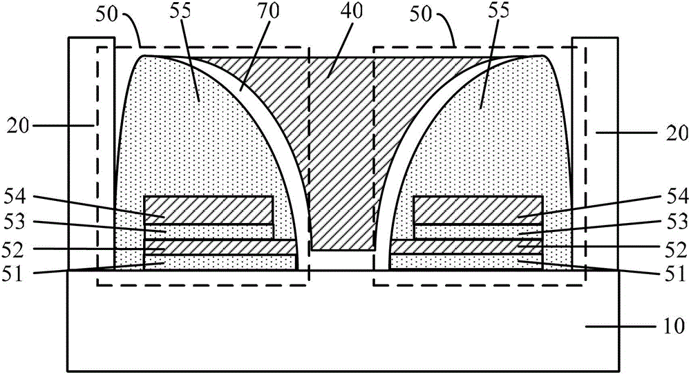
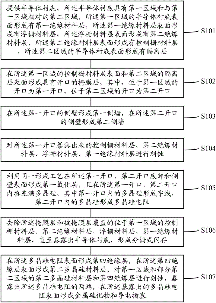
[0025] When the split-gate flash memory and the polysilicon resistor are formed by the existing process, the split-gate flash memory and the polysilicon resistor are manufactured separately, that is, the split-gate flash memory is formed in a designated area, and then the split-gate flash memory A mask layer is formed on the surface, and then polysilicon resistors are formed in other areas. However, since the production of the split-gate flash memory requires the deposition of multiple polysilicon layers to form control gates, floating gates or word lines, after the split-gate flash memory is formed, the multi-layer polysilicon layers in other regions are etched away, and then Forming another polysilicon layer to make polysilicon resistors causes waste of materials and increases in process steps.

[0026] Therefore, the embodiment of the present invention provides a method for forming a semiconductor integrated device. A first sidewall is formed on the sidewall of a first opening...


PUM


Abstract

A formation method of a semiconductor integrated device includes: forming a first opening in a mask layer in a first region, forming a second opening in the mask layer in a second region, forming a first sidewall on the side wall of the first opening, forming a second sidewall on the side wall of the second opening, fully filling the first opening and the second opening with polycrystalline silicon by same process, forming word lines of a split-gate flash memory with the polycrystalline silicon in the first opening, and forming a polysilicon resistor with the polycrystalline silicon in the second opening. Therefore, the polysilicon resistor is formed while the split-gate flash memory is formed, no extra process is added, and cost of production process is reduced.

Description

technical field [0001] The invention relates to semiconductor technology, in particular to a method for forming a semiconductor integrated device. Background technique [0002] As the feature size (CD, Critical Dimension) of semiconductor devices becomes smaller and smaller, the integration of semiconductor chips becomes higher and higher, and the number and types of devices that need to be formed per unit area are also increasing, thus affecting the semiconductor process. requirements are also getting higher. How to rationally arrange the positions of various devices, and how to save semiconductor process steps and materials by using the common points of each device manufacturing has become a hot research topic. [0003] In the manufacture of semiconductor devices, polysilicon is a very commonly used conductive material, which can usually be used to make gate electrodes of MOS transistors, high resistance polysilicon resistors, floating gates of flash memory, control gates...

Claims


Application Information

Patent Timeline
IPC IPC(8): H01L21/8247
Inventor 江红
Owner SHANGHAI HUAHONG GRACE SEMICON MFG CORP
Why Eureka
Try Eureka