LED display screen package process based on COB (chip on board) technology and LED display screen

A technology of LED display and packaging technology, which is applied in the direction of identification devices, instruments, electrical components, etc., can solve problems such as difficult to produce LED displays with higher pixels, achieve overall performance and quality improvement, improve heat dissipation, and increase pixels Effect

Active Publication Date: 2013-04-03
SHENZHEN JIUZHOU OPTOELECTRONICS TECH
View PDF3 Cites 28 Cited by
  • Summary
  • Abstract
  • Description
  • Claims
  • Application Information

AI Technical Summary

Problems solved by technology

At present, the distance between adjacent pixels on most LED displays is 4mm, 3mm or 2.5mm, and mass production has begun. However, with the rapid development of LED display technology, people put forward higher requirements for the pixels of LED displays. , and the LED display screens on the market can no longer meet the above requirements, and it is difficult to produce LED display screens with higher pixels by conventional packaging methods

Method used


Image

  • LED display screen package process based on COB (chip on board) technology and LED display screen
  • LED display screen package process based on COB (chip on board) technology and LED display screen
  • LED display screen package process based on COB (chip on board) technology and LED display screen

Examples


Embodiment Construction

[0022] The present invention will be described in more detail below in conjunction with the accompanying drawings and embodiments.

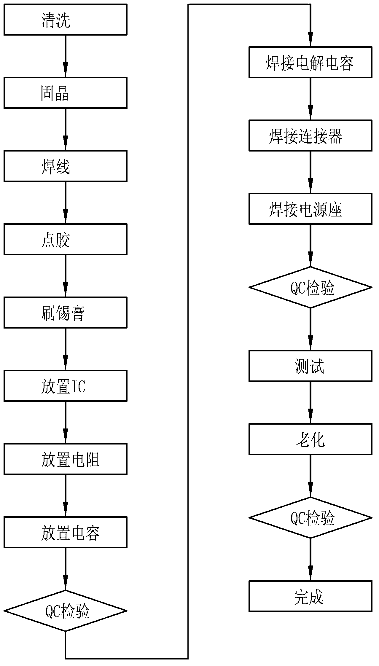
[0023] The invention discloses an LED display packaging process based on COB technology, which combines Figure 1 to Figure 4 As shown, it includes the following steps:

[0024] a. Clean PCB1 with a plasma machine, the cleaning conditions are argon 10sccm, vacuum pressure 180mTorr, plasma time 5s;

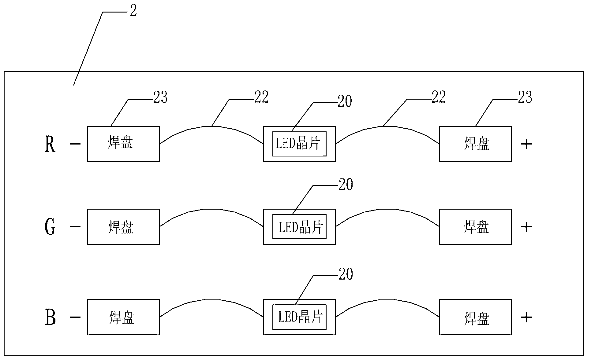
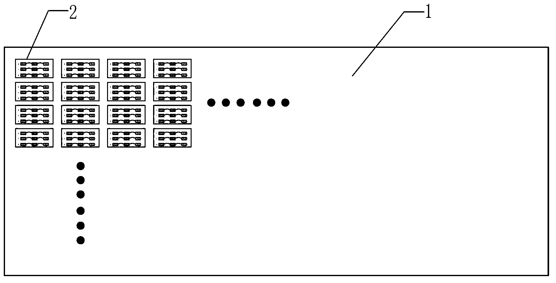
[0025] b. Use a crystal expander to evenly expand a plurality of LED chips 20, and every three LED chips 20 form a point light source 2, and the distance between two adjacent point light sources 2 is <2mm;

[0026] c. Fix the LED chip 20 on the PCB1 with silver glue, and then use red light to solidify the crystal. The conditions for the solidification of the crystal are: the temperature is set to 160±5°C, and the baking time is 2h; then red light, green light and blue light are used to solidify crystal, the crystal-bonding conditions are: the temper...


PUM


Abstract

The invention discloses an LED display screen package process based on COB (chip on board) technology. The package process includes the steps: a, cleaning a PCB (printed circuit board) by a plasma machine; b, evenly spreading a plurality of LED wafers by a semiautomatic die-spread; c, fixing the LED wafers on the PCB by silver colloid and then carrying out die bonding; d, welding gold wires among the LED wafers and a pad by a wire bonding machine; e, dispensing the LED wafers by a dispenser; f, brushing tin paste for the PCB, placing an IC (integrated circuit), a resistor and a capacitor, welding the IC, the resistor and the capacitor on the PCB by a reflow welder and then manually welding an electrolytic capacitor, a power socket and a connection terminal on the PCB; and g, performing power-on test for an LED display screen and aging the LED display screen in a heat-circulation oven after the test is correct. Each three LED wafers form a point light source, and the distance between each two point light sources is 2mm. By the aid of the package process, the LED display screen can have higher pixels.

Description

technical field [0001] The present invention relates to the technical field of LED display packaging, in particular to an LED display packaging process and LED display based on chip on board (COB) technology. Background technique [0002] With the gradual maturity of LED display technology, people have higher and higher requirements for the clarity of LED display screens, making high-definition LED display screens popular on a large scale. At present, the distance between adjacent pixels on most LED displays is 4mm, 3mm or 2.5mm, and mass production has begun. However, with the rapid development of LED display technology, people have put forward higher requirements for the pixels of LED displays. , and the LED display screens on the market can no longer meet the above requirements, and it is difficult to produce LED display screens with higher pixels by conventional packaging methods. Contents of the invention [0003] The technical problem to be solved by the present inv...

Claims


Application Information

Patent Timeline
Patent Type & Authority Applications(China)
IPC IPC(8): H01L33/48H01L33/64G09F9/33
Inventor 梁正恺郭伦春陈艳宋琦徐劲绘张铁钟
Owner SHENZHEN JIUZHOU OPTOELECTRONICS TECH
Why Eureka
Try Eureka