Common image surface imaging method based on CMOS (complementary metal oxide semiconductor) package

An imaging method and imaging technology, which are applied in the directions of image communication, color TV parts, TV system parts, etc., can solve the problem of increasing system complexity, poor imaging effect at the junction between image planes, and inability to realize system miniaturization design. requirements, etc., to avoid the poor junction of the imaging area and avoid the effect of the image effect

Inactive Publication Date: 2013-04-03
TIANJIN UNIV
View PDF5 Cites 10 Cited by
  • Summary
  • Abstract
  • Description
  • Claims
  • Application Information

AI Technical Summary

Problems solved by technology

[0004] The first method is difficult to meet the real-time application requirements of common image plane imaging stereo vision detection due to the single photosensitive area structure of ordinary CIS; the second method cannot be realized due to the increase of system complexity due to the use of multiple CIS The miniaturization design requirements of the system; the third method has poor imaging effect at the junction between the divided image planes due to the physical edge of each lens in the optical path

Method used


Image

  • Common image surface imaging method based on CMOS (complementary metal oxide semiconductor) package
  • Common image surface imaging method based on CMOS (complementary metal oxide semiconductor) package
  • Common image surface imaging method based on CMOS (complementary metal oxide semiconductor) package

Examples


Embodiment Construction

[0026] In order to make the purpose, technical solution and advantages of the present invention clearer, the implementation manners of the present invention will be further described in detail below.

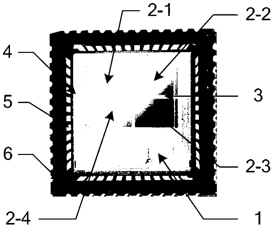
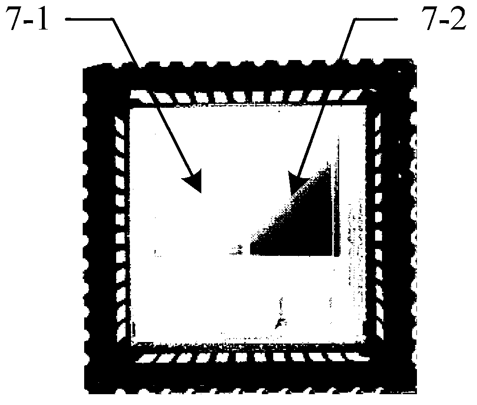
[0027] see figure 1 and Figure 4 , in order to meet the requirements for real-time detection applications and system miniaturization design, and improve the imaging effect at the junction of the segmented image planes, an embodiment of the present invention provides a common image plane imaging method based on CMOS packaging, see the following description for details:

[0028] 101: Carry out partitioned imaging layout on the imaging sensing area of ​​the photosensitive chip 1, divide it into at least two imaging sensing areas 2, adjacent imaging sensing areas 2 are separated from each other by a spacer area 3, and each imaging sensing area 2 corresponds to an optical sensing area 2 Channels, different scene information or different spectral information of the same scene are si...


PUM


Abstract

The invention discloses a common image surface imaging method based on CMOS (complementary metal oxide semiconductor) package. Partition imaging layout is performed on imaging induction areas of a light induction chip, the light induction chip is divided into at least two imaging induction areas, the adjacent imaging induction areas are separated from each other by a spacer, each imaging induction area corresponds to an optical channel, different scene information or different spectral information of the same scene is simultaneously imaged on the light induction chip by respectively independent optical channels, the light induction chip is connected with an internal lead bonding area of a substrate dam through a gold wire, photoelectric conversion processes of pixels of the imaging induction areas are mutually independent, and photoelectric conversion signals of the imaging induction areas are uniformly processed by a peripheral support circuit. The method meets the integral structure design requirements of system microminiaturization on size and volume, the requirement of instantaneity of stereoscopic vision imaging is met, and poor imaging effects of imaging area junctions caused by image surface division completely depending on multiple optical paths are avoided.

Description

technical field [0001] The invention relates to a common image plane imaging method, in particular to a common image plane imaging method based on CMOS packaging. Background technique [0002] Common image plane imaging bionic stereo vision needs to acquire multiple images for splicing and processing. To obtain multiple image information, there are three existing technologies: one is to use a single CIS (CMOS image sensor) to shoot in time series; the second is to use multiple CISs to simultaneously collect images; the third is to rely entirely on multiple optical channels Perform common image plane imaging. [0003] In the process of realizing the present invention, the inventor finds that at least the following disadvantages and deficiencies exist in the prior art: [0004] The first method is difficult to meet the real-time application requirements of common image plane imaging stereo vision detection due to the single photosensitive area structure of ordinary CIS; the ...

Claims


Application Information

Patent Timeline
Patent Type & Authority Applications(China)
IPC IPC(8): H04N5/374H04N5/3745
Inventor 王向军于雅楠张为林琳刘峰
Owner TIANJIN UNIV
Why Eureka
Try Eureka