Plating cup with contoured cup bottom

A bottom surface, chip technology, applied in sealing devices, contact devices, electrolytic components, etc., can solve problems such as the corrosion characteristics of electroplating solutions and the difficulty in establishing electrical connections

Active Publication Date: 2013-04-10
NOVELLUS SYSTEMS
View PDF4 Cites 30 Cited by
  • Summary
  • Abstract
  • Description
  • Claims
  • Application Information

AI Technical Summary

Problems solved by technology

However, in certain configurations, the conductive seed layer on the substrate that is contacted by the electrical connection can become thinner towards the edge of the substrate, making it more

Method used


Image

  • Plating cup with contoured cup bottom
  • Plating cup with contoured cup bottom
  • Plating cup with contoured cup bottom

Examples


Embodiment Construction

[0027] In the following description, numerous specific details are set forth in order to provide a thorough understanding of presented concepts. The concepts presented herein may also be practiced without some or all of these specific details. In other instances, well known process operations have not been described in detail so as not to unnecessarily obscure the described concepts. While some concepts are described in connection with specific embodiments, it will be understood that these embodiments are not meant to be limiting.

[0028] introduce

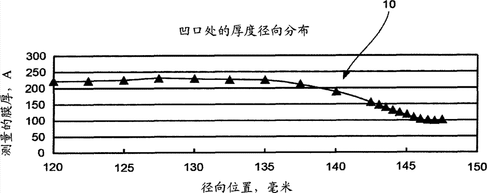
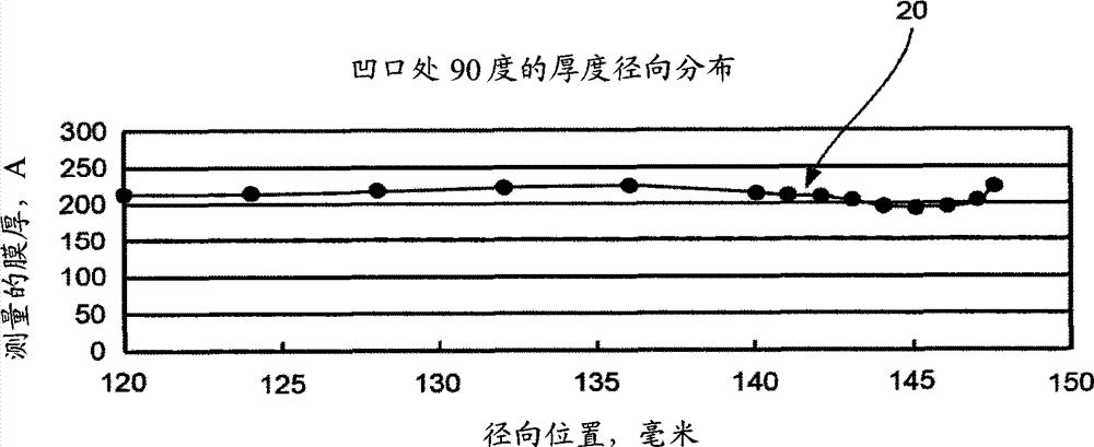
[0029] As the semiconductor industry moves towards the use of thinner seed layers in electroplating, the higher resistance of these thinner layers can affect various aspects of electroplating and in some cases cause defects in the electroplated layer. The resistance of the thinner seed layer is usually greater than 5 ohms / square, sometimes as high as about 30 ohms / square, and even about 40 ohms / square. Higher resistance can le...


PUM


Abstract

Disclosed herein are cups for engaging wafers during electroplating in clamshell assemblies and supplying electrical current to the wafers during electroplating. The cup can comprise an elastomeric seal disposed on the cup and configured to engage the wafer during electroplating, where upon engagement the elastomeric seal substantially excludes plating solution from a peripheral region of the wafer, and where the elastomeric seal and the cup are annular in shape, and comprise one or more contact elements for supplying electrical current to the wafer during electroplating, the one or more contact elements attached to and extending inwardly towards a center of the cup from a metal strip disposed over the elastomeric seal. A notch area of the cup can have a protrusion or an insulated portion on a portion of a bottom surface of the cup where the notch area is aligned with a notch in the wafer.

Description

[0001] Cross References to Related Applications [0002] This application claims the benefit of U.S. Provisional Application No. 61 / 533,779, filed September 12, 2011, entitled "PLATING CUP WITH CONTOURED CUP BOTTOM," Priority, which is hereby incorporated by reference in its entirety for all purposes. technical field [0003] The present invention relates to the formation of damascene interconnects for integrated circuits, and electroplating apparatus for use in the fabrication of integrated circuits. Background technique [0004] Electroplating is a common technique for depositing one or more layers of conductive metal in integrated circuit (IC) fabrication. In some fabrication processes, it is used to deposit single or multiple levels of copper interconnects between features of various substrates. An apparatus for electroplating typically includes an electroplating cell having an electrolyte pool / bath and a clamshell designed to hold the semiconductor substrate during el...

Claims


Application Information

Patent Timeline
IPC IPC(8): C25D7/12H01L21/288
CPCC25D7/123C25D17/001C25D17/004C25D17/005C25D17/007C25D17/06C25D7/126C25D17/12
Inventor 何志安冯敬斌尚蒂纳特·古艾迪弗雷德里克·D·威尔莫特
Owner NOVELLUS SYSTEMS
Why Eureka
Try Eureka