Liquid crystal display substrate and preparation method thereof and liquid crystal display device
A liquid crystal display device and liquid crystal display technology, applied in nonlinear optics, instruments, optics, etc., can solve the problems of difficult miniaturization and narrow frame design of liquid crystal display devices, and achieve easy miniaturization and narrow frame design, and realize miniaturization And narrow frame design, the effect of uniform overall thickness
- Summary
- Abstract
- Description
- Claims
- Application Information
AI Technical Summary
Problems solved by technology
Method used
Image
Examples
Embodiment 1
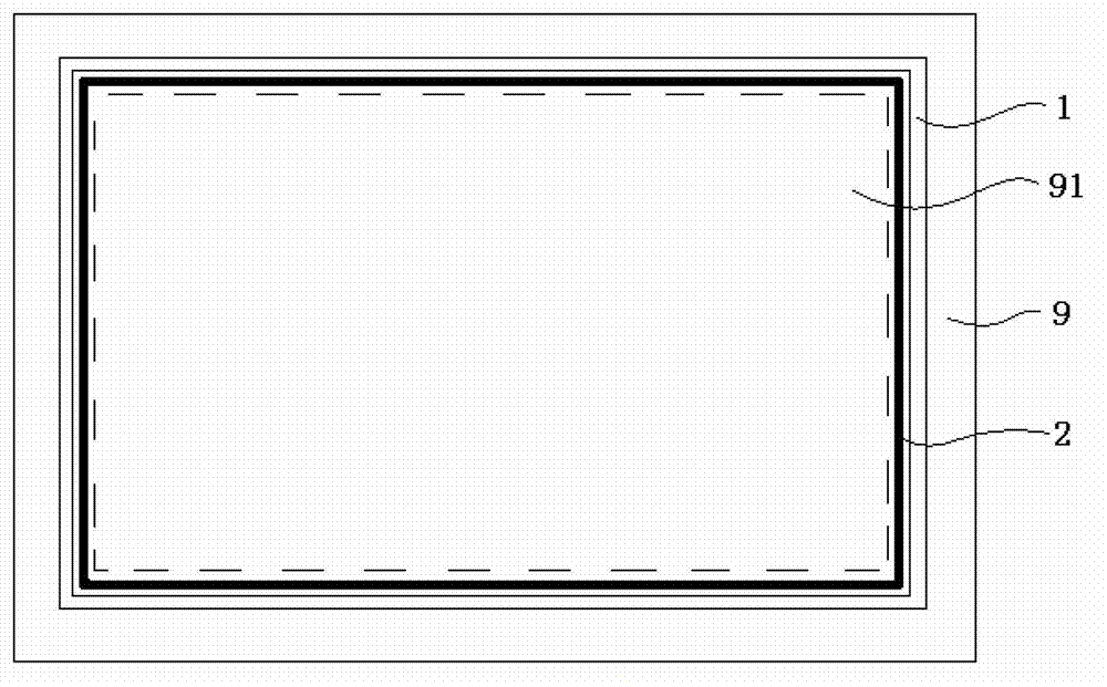
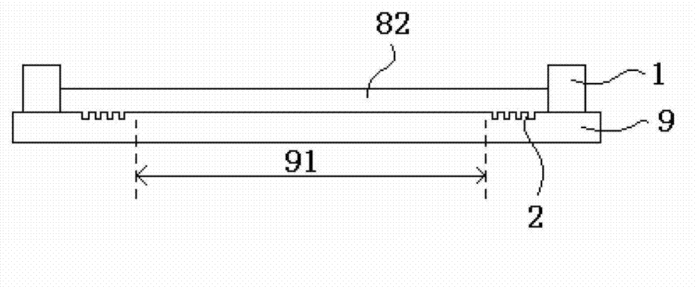
[0030] This embodiment provides a liquid crystal display substrate, which includes a substrate and an alignment film disposed on the substrate, the substrate has a display area for displaying; the substrate is provided with a retaining wall located at the periphery of the display area; the alignment film covers the display area, And the outer edge is in contact with the retaining wall, and the thickness of the alignment film is less than or equal to the height of the retaining wall.
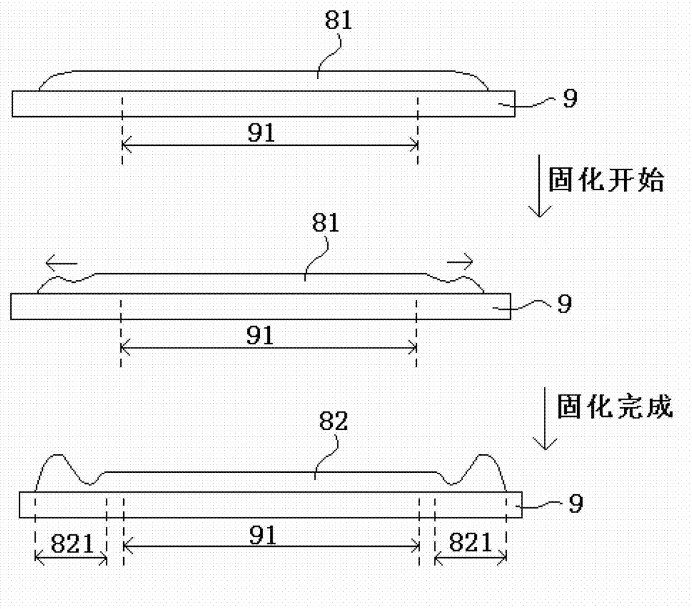
[0031] In the liquid crystal display substrate of this embodiment, a retaining wall is provided on the periphery of the display area. When the alignment liquid is applied to the substrate, its outer edge is in contact with the retaining wall, so that the edge will not form an arc or a very large arc due to tension. Therefore, the overall thickness of the alignment film formed after curing is uniform, and there is no Halo region or the Halo region is very small, which is beneficial to the miniaturi...
Embodiment 2
[0033] Such as Figure 2 to Figure 4 As shown, this embodiment provides a liquid crystal display substrate, which includes a substrate 9 and an alignment film 82 disposed on the substrate 9 .
[0034] Preferably, the liquid crystal display substrate is an array substrate or a color filter substrate.
[0035] The above-mentioned "substrate 9 of the liquid crystal display substrate" includes a substrate (such as a glass substrate) and other structures formed on the substrate; for an array substrate, the substrate 9 may include structures such as a thin film transistor array, pixel electrodes, and leads; for a color filter The substrate, the substrate 9 may include structures such as a color filter, a common electrode, and a black matrix. Since the specific structure in the substrate 9 can be in many different known forms (for example, the color filter can also be located on the array substrate), it will not be described in detail here, nor shown in the figure.
[0036] Since t...
Embodiment 3
[0058] This embodiment provides a method for preparing a liquid crystal display substrate, which includes:
[0059] The alignment liquid is applied on the substrate of the liquid crystal display substrate of any one of the above embodiments, so that the alignment liquid covers the display area and the outer edge contacts the barrier wall, and the thickness of the alignment liquid layer is less than or equal to the height of the barrier wall.
[0060] heating to solidify the alignment liquid to form an alignment film.
[0061] Since the method for preparing the liquid crystal display substrate of this embodiment uses a substrate with a barrier wall, the above-mentioned liquid crystal display substrate is prepared, and the alignment film does not have a Halo region or the Halo region is very small, so it is easy to realize Miniaturization and narrow bezel design of liquid crystal display devices.
PUM
| Property | Measurement | Unit |
|---|---|---|
| Height | aaaaa | aaaaa |
Abstract
Description
Claims
Application Information


