Transparent conductive film
A technology of transparent conductivity and transparent conductor, applied in the direction of conductive layer, circuit, printed circuit, etc. on insulating carrier
- Summary
- Abstract
- Description
- Claims
- Application Information
AI Technical Summary
Problems solved by technology
Method used
Image

Examples
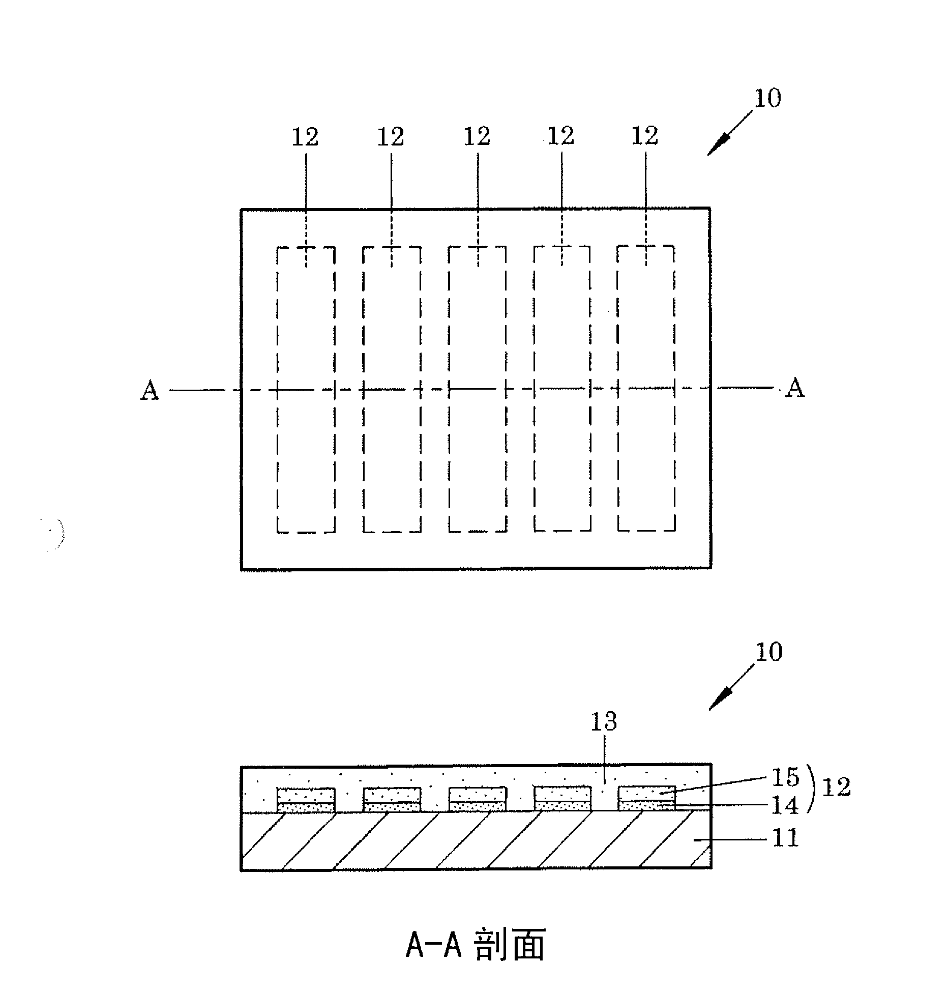
Embodiment 1
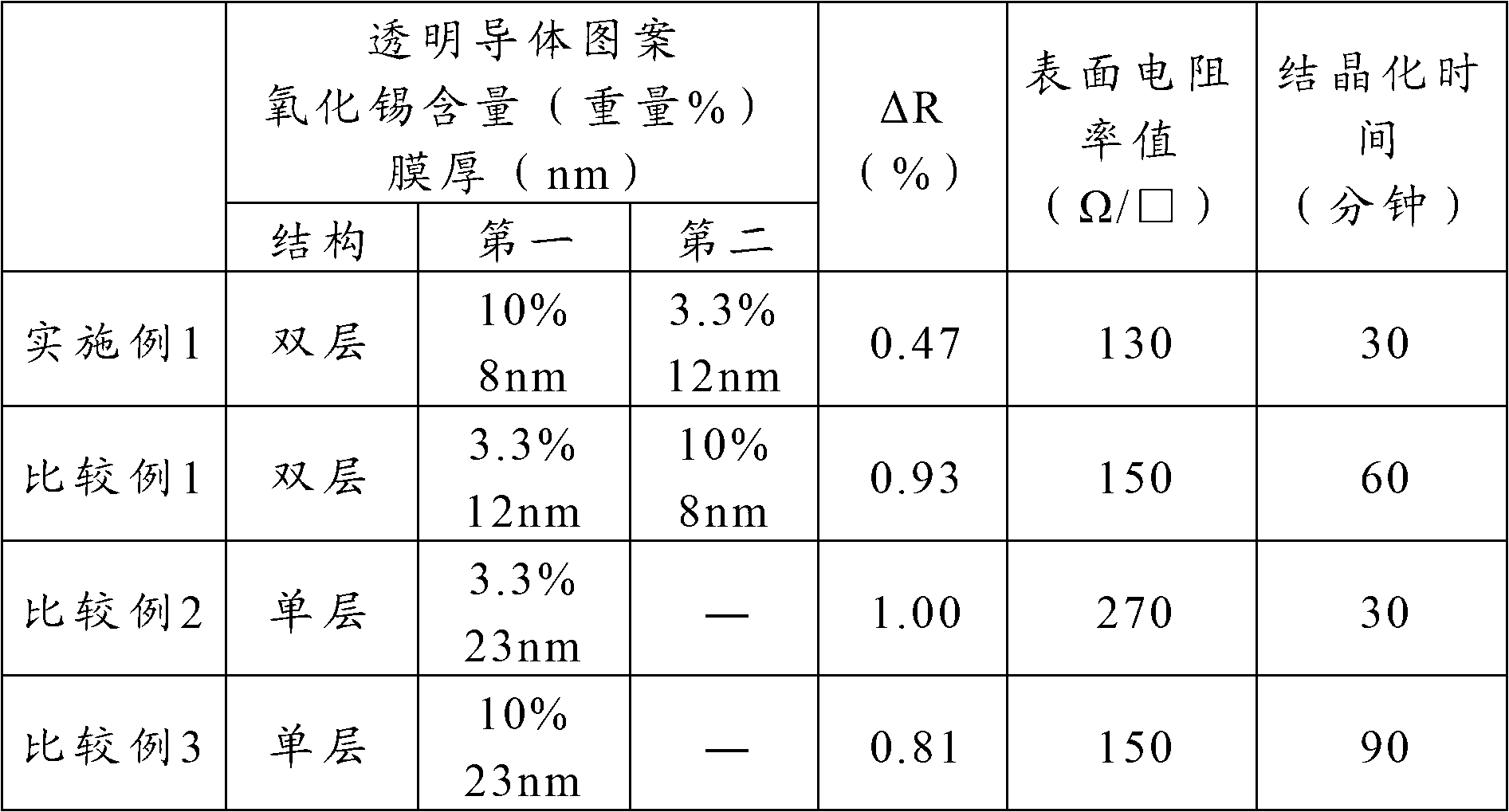
[0048] A primer layer (thickness 30 nm) of a thermosetting resin containing melamine resin was formed on a polyethylene terephthalate film having a thickness of 23 μm, and the film substrate 11 was prepared. The roll of the film substrate 11 is set in a sputtering device. The atmosphere in the sputtering device is a pressure of 0.4 Pa, and the specific composition of the gas is 80% by volume of argon and 20% by volume of oxygen. While unwinding the roll of the film substrate 11 at a certain speed, the first amorphous layer of indium tin oxide and the second amorphous layer of indium tin oxide are sequentially formed on the film substrate 11 to form a thickness of 20 nm Transparent conductor film. For the first amorphous layer of indium tin oxide, the content of tin oxide is 10% by weight and the thickness is 8 nm. For the second amorphous layer of indium tin oxide, the content of tin oxide is 3.3% by weight and the thickness is 12 nm. The film substrate 11 on which the first...
PUM
| Property | Measurement | Unit |
|---|---|---|
| thickness | aaaaa | aaaaa |
| thickness | aaaaa | aaaaa |
| thickness | aaaaa | aaaaa |
Abstract
Description
Claims
Application Information