
Shaping method of inductance element

A technology of inductance components and forming methods, applied in electrical components, inductance/transformer/magnet manufacturing, circuits, etc., can solve the problems of difficulty in reducing volume, reducing the number of turns of coil A1, and increasing cost, and achieve high permeability and low loss. , the effect of reducing the volume thickness

Inactive Publication Date: 2013-04-10
AJOHO ENTERPRISE
View PDF5 Cites 4 Cited by
  • Summary
  • Abstract
  • Description
  • Claims
  • Application Information

AI Technical Summary

Problems solved by technology

[0004] And the inductance element can be divided into wire-wound type and multi-layer type according to the structure. Among them, the wire-wound type is the most commonly used technology, because it has the advantages of small loss, large allowable current, simplicity, and low cost. However, its structure is restricted. However, according to electromagnetic theory, coils are used to wind iron cores to form inductance components. Most traditional inductance components are produced by winding wires. The thickness of the coils can be used to control the degree of current resistance. The number of windings is used to adjust the inductance value. The design has a large flexible space, but the biggest disadvantage is that the size is not easy to shrink.
[0005] In the traditional method of manufacturing inductance components from iron-silicon alloys, the inductance components are formed by means of assembly by using flake or block iron-silicon alloy materials. Please refer to Figure 13 As shown, it is a side view sectional view of the existing inductance element. In the conventional inductance element A, a sheet or block-shaped iron-silicon alloy material A2 is assembled outside the coil A1, and the iron-silicon alloy material A2 is inside, The outer surface is formed with an insulating layer A3, which must be processed by dispensing and bonding during assembly, but the operation steps are cumbersome and complicated, resulting in increased costs; in addition, the inductance element A is formed by assembly, and the coil A1 is fitted through the through hole A11 In the iron-silicon alloy material 2, it is inevitable that there is a gap A4 between the coil A1 and the iron-silicon alloy material A2, and it is easy to form a larger magnetic path (Le) on the periphery of the coil A1, and in the through hole of the coil A1 The inner circumference of A11 is affected by the gap A4, resulting in a smaller cross-sectional area. Even if the coil A1 causes a large electromagnetic rate loss, the traditional inductance element A cannot reduce the number of turns of the coil A1, nor can it be too thin The coil A1 relatively increases the material burden and cost
[0006] In this way, how to solve the problems and defects of the existing inductive elements such as large loss of electromagnetic rate, difficult reduction in size, and cost increase due to the use of coil materials is what the inventor and related manufacturers engaged in this industry are eager to study. , the direction of improvement

Method used


Image

  • Shaping method of inductance element
  • Shaping method of inductance element
  • Shaping method of inductance element

Examples


Embodiment Construction

[0040] In order to achieve the above-mentioned purpose and effect, the technical means and the structure thereof adopted in the present invention are described in detail with respect to the preferred embodiments of the present invention.

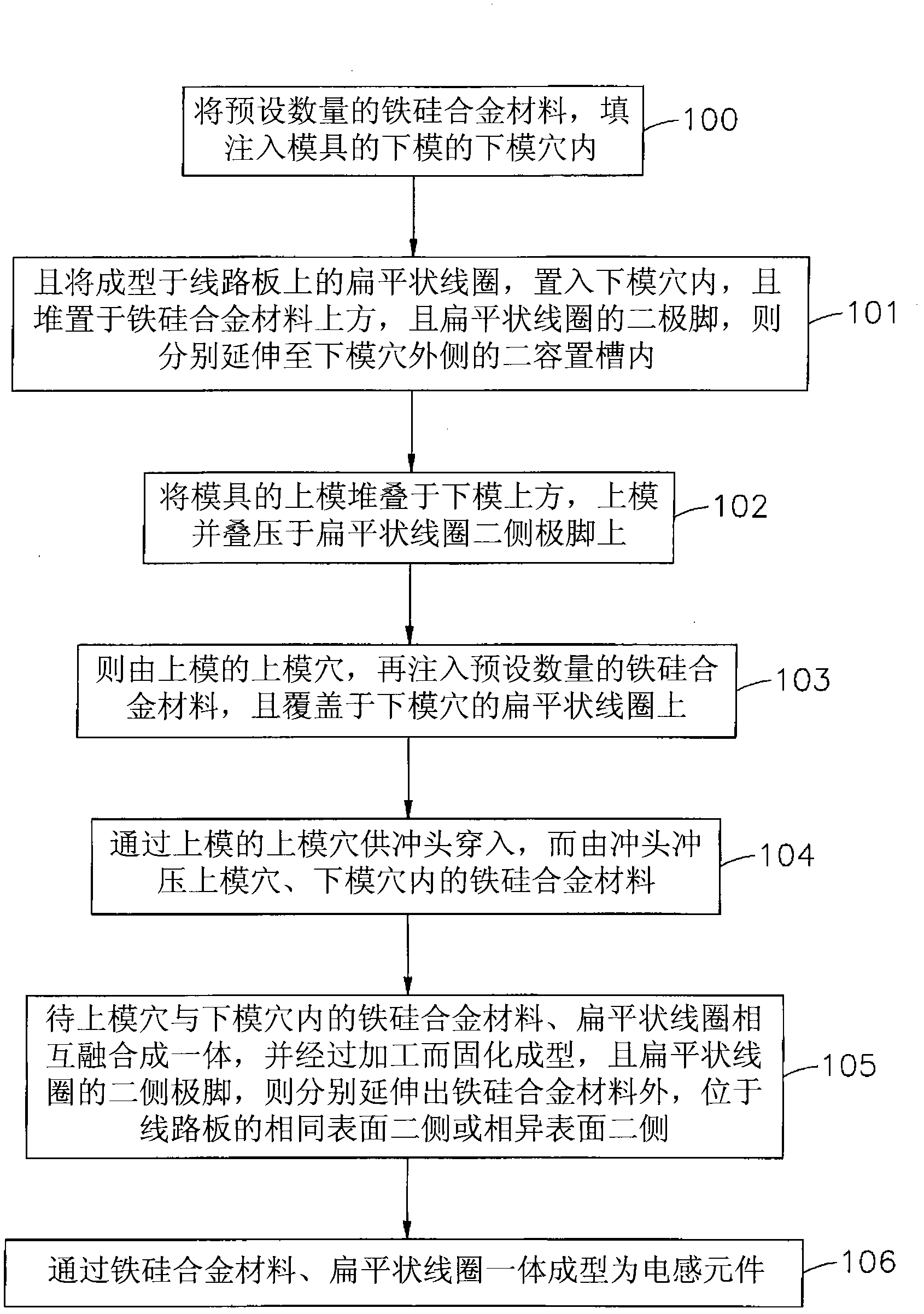
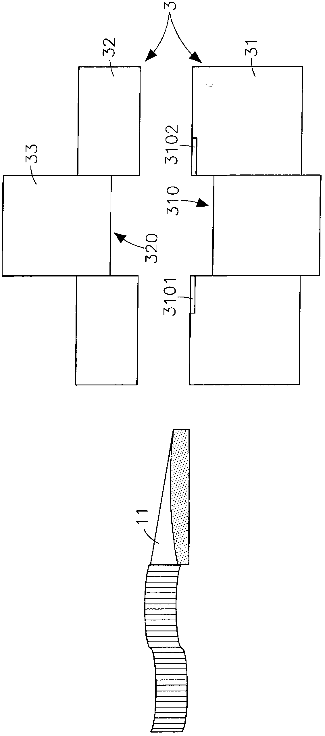
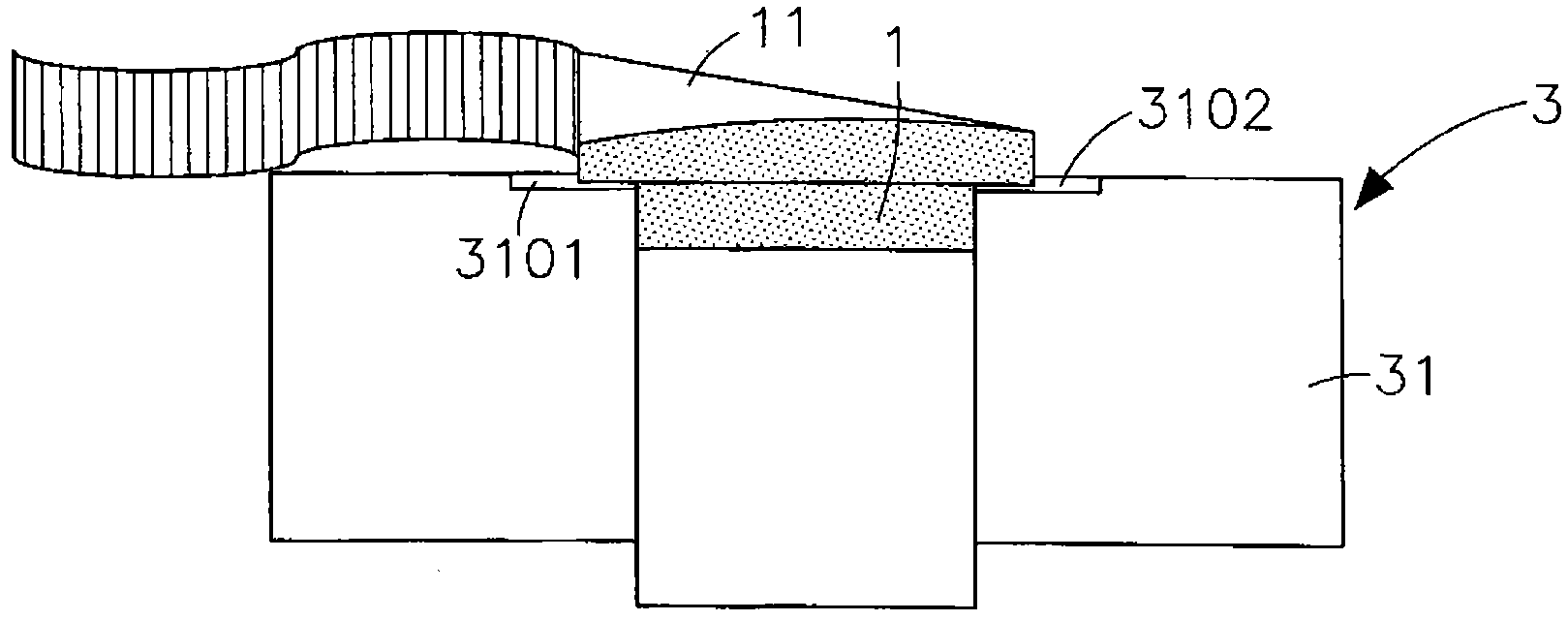
[0041] Please refer to shown in sudden 1, 2, 3, 4, 5, 6, 7, 8, it is the manufacturing flow chart of the present invention, the processing operation side view (one), the processing operation side view (two), the processing operation side view ( Three), processing operation side view (four), processing operation side view (five), processing operation side view (six), the three-dimensional appearance diagram of flat coil, can clearly find out by shown in the figure, the inductance element of the present invention Including iron-silicon alloy material 1 and coil 2, the steps of processing and forming are as follows:

[0042] (100) Fill a predetermined amount of FeSi alloy material 1 into the lower mold cavity 310 of the lower mold 31 of the mol...


PUM


Abstract

The invention provides a shaping method of an inductance element. The shaping method comprises the following steps of: filling moderate iron-silicon alloy materials in lower die cavities of lower dies of a mold; stacking flat coils shaped on a circuit board on the iron-silicon alloy materials of the lower die cavities, wherein two polar pins of the flat coils respectively extend to two containing slots at the external side; stacking upper dies above the lower dies and overlapping the upper dies on the two side polar pins; filling moderate iron-silicon alloy materials in upper die cavities of the upper dies so as to cover the flat coils and penetrate through the upper die cavities through punching heads; punching the iron-silicon alloy materials in the upper die cavities and the lower die cavities, so as to integrate the iron-silicon alloy materials and the flat coils into one; and processing, curing and shaping to shape the inductance element. The size thickness of the inductance element is reduced by the flat coils; and the inductance element with low energy consumption and high magnetic permeability is shaped.

Description

technical field [0001] The present invention designs a molding method for inductive elements, especially a molding method for forming thin-shaped inductive elements with good magnetic conduction effect. The upper and lower mold cavities are respectively filled with iron-silicon alloy materials and flat coils, and then stamped and extruded. , After curing and forming, the thickness of the inductance element will be reduced, and the overall volume will be reduced, but it has good magnetic permeability. Background technique [0002] Among many electronic components, the inductance element is auxiliary in nature, and its main function is to hinder the change of current to maintain the stability of the electronic product. The structure of the inductance element can be designed according to the application circuit. Different structures, and in The currently commonly used inductance components are roughly divided into two types of application modes. One is for signal purposes, such...

Claims


Application Information

Patent Timeline
Patent Type & Authority Applications(China)
IPC IPC(8): H01F41/00H01F41/06H01F27/28H01F41/074
Inventor 莫家平
Owner AJOHO ENTERPRISE
Learn More