Epitaxial wafer manufacturing method suitable for super junction device

A manufacturing method and technology of epitaxial wafers, applied in semiconductor/solid-state device manufacturing, electrical components, circuits, etc., can solve problems such as poor BV uniformity and inconsistent concentration ratio distribution, and achieve the effect of improving uniformity

Active Publication Date: 2015-04-08
SHANGHAI HUAHONG GRACE SEMICON MFG CORP
View PDF6 Cites 0 Cited by
  • Summary
  • Abstract
  • Description
  • Claims
  • Application Information

AI Technical Summary

Problems solved by technology

Therefore, the concentration ratio distribution of the P-type epitaxial layer 102 whose resistivity distribution is high in the center and low at the edge and the N-type epitaxial layer 101 whose resistivity is distributed along the lines are inconsistent, resulting in poor BV uniformity.

Method used


Image

  • Epitaxial wafer manufacturing method suitable for super junction device
  • Epitaxial wafer manufacturing method suitable for super junction device
  • Epitaxial wafer manufacturing method suitable for super junction device

Examples


Embodiment Construction

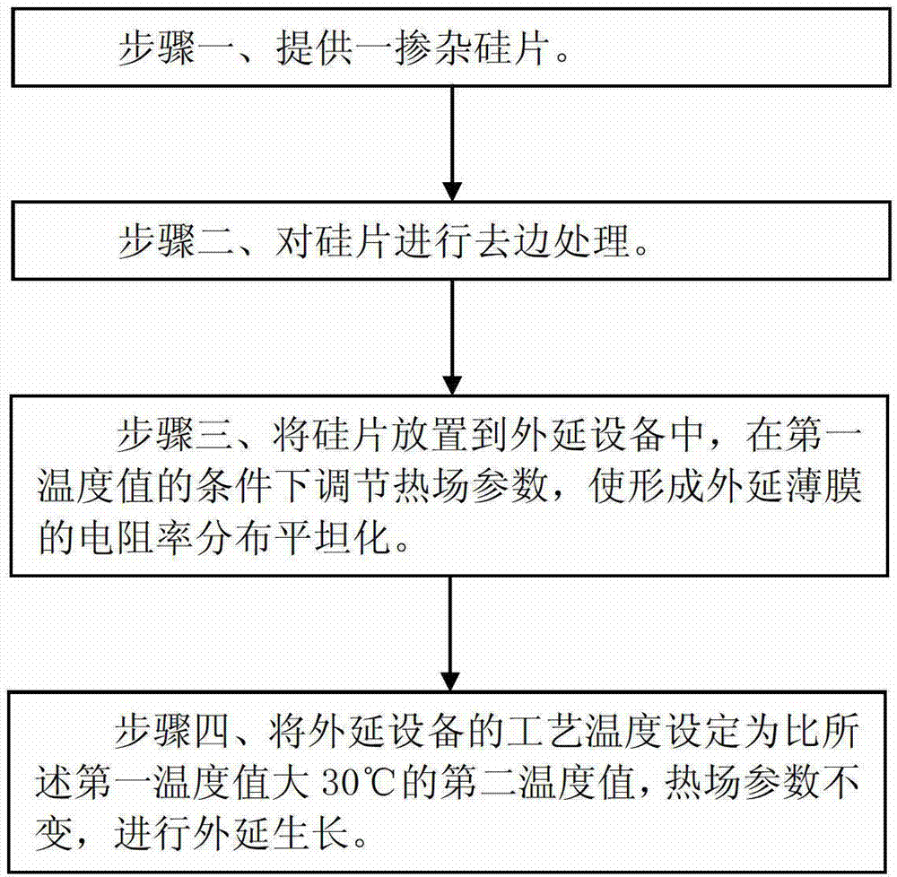
[0023] Such as image 3 Shown is the flow chart of the embodiment of the present invention; Figure 4 Shown is a schematic diagram of the resistivity distribution of the epitaxial wafer produced by the method of the embodiment of the present invention. The embodiment of the present invention is applicable to the epitaxial wafer manufacturing method of the super junction device including steps:

[0024] Step 1. Provide a silicon wafer, the doping type of the silicon wafer is the same as that of the epitaxial layer 1 to be formed later and both are N-type, and the doping concentration of the silicon wafer is higher than that of the epitaxial layer 1 to be formed later. The doping concentration of the epitaxial layer.

[0025] Step 2. De-edge treatment is performed on the silicon wafer, the de-edge treatment is used to remove the thermal oxide layer at the back edge of the silicon wafer, and the de-edge treatment is 2 mm. The edge removal process specifically includes: coverin...


PUM


Abstract

The invention discloses an epitaxial wafer manufacturing method suitable for a super junction device. The epitaxial wafer manufacturing method suitable for the super junction device comprises the steps of providing a doping silicon wafer, carrying out edge-removing treatment to the silicon wafer, placing the silicon wafer in an epitaxial device, regulating thermal field parameters at the condition of a first temperature value, enabling resistivity of a formed epitaxial thin film to be distributed evenly, setting the process temperature of the epitaxial device as a second temperature value which is 30 degrees higher than the first temperature value, enabling the thermal field parameters not to be changed, and carrying out epitaxial growth. The epitaxial wafer manufacturing method suitable for the super junction device is capable of enabling resistivity of the epitaxial wafer to be distributed in a concentric circle mode, and therefore evenness of breakdown voltage of the super junction device which adopts a groove filling process is improved.

Description

technical field [0001] The invention relates to a semiconductor integrated circuit manufacturing process method, in particular to an epitaxial wafer manufacturing method suitable for super-junction (super-junction) devices. Background technique [0002] Such as figure 1 As shown, it is a schematic cross-sectional view of the P-type and N-type thin layers of the existing super-junction device; the existing super-junction device adopts trench filling technology, and the structure of the P-type and N-type thin layers includes: N-type epitaxial layer 101 A groove is formed on the N-type epitaxial layer 101, and a P-type epitaxial layer 102 is filled in the groove. The thin N-type epitaxial layer 101 between the P-type epitaxial layers 102 constitutes the P-type and N-type thin layers of the super junction device. [0003] For the P-type epitaxial layer 102 filled in the trench, due to the limitations of epitaxial process equipment and process methods, the resistivity distribut...

Claims


Application Information

Patent Timeline
Patent Type & Authority Patents(China)
IPC IPC(8): H01L21/20H01L21/22
Inventor 张洪伟董颖
Owner SHANGHAI HUAHONG GRACE SEMICON MFG CORP
Why Eureka
Try Eureka