Light-emitting diode

一种发光二极管、电极的技术,应用在纳米光学、半导体器件、电气元件等方向,能够解决光取出效率低、发光二极管不利、耗散等问题,达到提高取出效率、提高出光效率、减小损耗的效果

Active Publication Date: 2013-04-10
TSINGHUA UNIV +1
View PDF5 Cites 3 Cited by
  • Summary
  • Abstract
  • Description
  • Claims
  • Application Information

AI Technical Summary

Problems solved by technology

[0004] However, the light extraction efficiency of existing light-emitting diodes (light extraction efficiency usually refers to the efficiency at which the light generated in the active layer is released from the inside of the light-emitting diode) is low, mainly due to the semiconductor (usually gallium nitride) The refractive index is greater than that of air, and the large-angle light from the active layer is totally reflected at the interface between the semiconductor and the air, so that most of the large-angle light is confined inside the light-emitting diode until it is dissipated by heat, etc.
This is very bad for light emitting diodes

Method used


Image

  • Light-emitting diode
  • Light-emitting diode
  • Light-emitting diode

Examples


Embodiment Construction

[0023] In order to further illustrate the present invention, the following specific embodiments are given and described in detail with accompanying drawings.

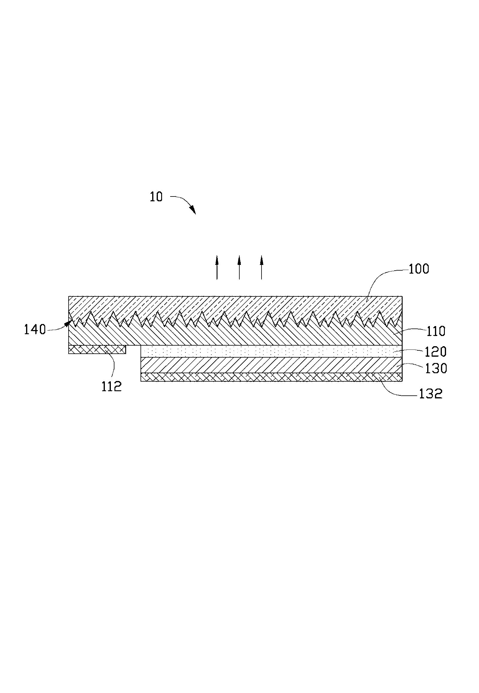
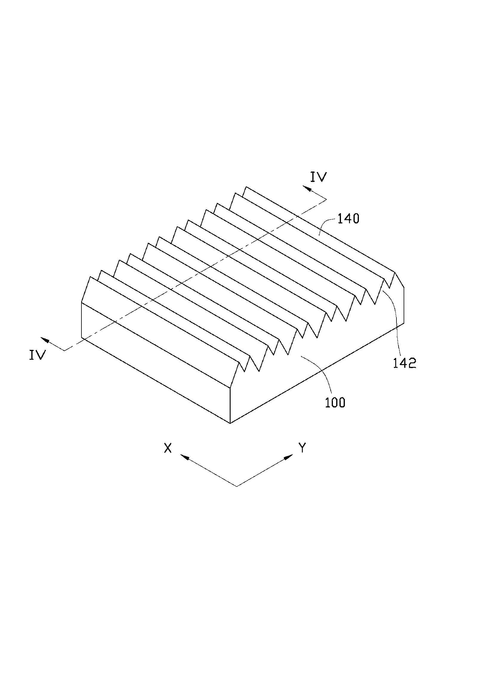
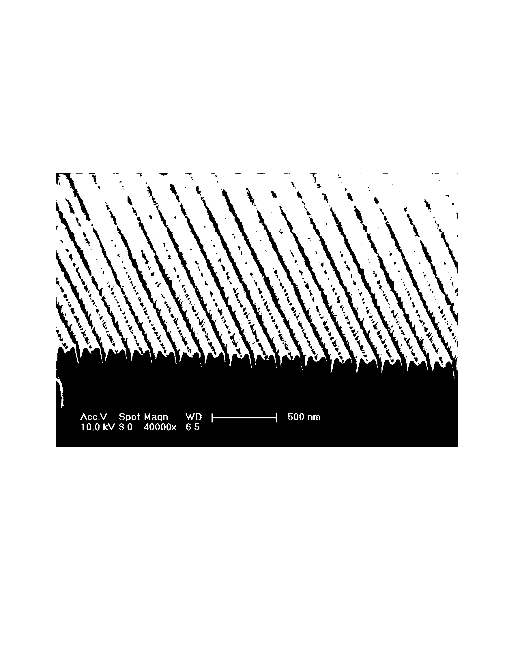
[0024] see figure 1 , the first embodiment of the present invention provides a light emitting diode 10, which includes: a substrate 100, a first semiconductor layer 110, an active layer 120, a second semiconductor layer 130, a first electrode 112, a second electrode 132 and a three-dimensional nanostructure array 140 . The substrate 100 has opposite first surface (not marked) and second surface (not marked), the first semiconductor layer 110 , active layer 120 and second semiconductor layer 130 are sequentially stacked on the first surface of the substrate 100 One side, and the first semiconductor layer 110 is disposed close to the substrate 100, the three-dimensional nanostructure array 140 is disposed on the surface of the substrate 100 adjacent to the first semiconductor layer 110, and the substrate 100 is far away ...


PUM


Abstract

The invention discloses a light-emitting diode which comprises a substrate, a first semiconductor layer, an active layer and a second semiconductor layer, wherein the substrate has a first surface and a second surface which are opposite to each other, the first semiconductor, the active layer and the second semiconductor are sequentially stacked on the first surface of the substrate, a first electrode is electrically connected with the first semiconductor layer, a second electrode is electrically connected with the second semiconductor, and the second surface of the substrate is a light-emitting surface of the light-emitting diode. At least one surface of the substrate further comprises a plurality of three-dimensional nanometer structures which extend parallelly, each three-dimensional nanometer structure comprises a first protruding edge and a second protruding edge which extend parallelly, a first groove is arranged between the adjacent first protruding edge and second protruding edge, a second groove is arranged between the adjacent three-dimensional nanometer structures, and the depth of the first groove is smaller than that of the second groove.

Description

technical field [0001] The invention relates to a light-emitting diode, in particular to a light-emitting diode with a three-dimensional nanostructure array. Background technique [0002] High-efficiency blue, green, and white light-emitting diodes made of gallium nitride semiconductor materials have remarkable features such as long life, energy saving, and environmental protection. They have been widely used in large-screen color displays, automotive lighting, traffic signals, multimedia displays, and optical communications. And other fields, especially in the field of lighting has broad development potential. [0003] A traditional light-emitting diode usually includes an N-type semiconductor layer, a P-type semiconductor layer, an active layer disposed between the N-type semiconductor layer and the P-type semiconductor layer, and a P-type electrode (usually a transparent electrode) disposed on the P-type semiconductor layer. and an N-type electrode disposed on the N-type...

Claims


Application Information

Patent Timeline
Patent Type & Authority Applications(China)
IPC IPC(8): H01L33/20H01L33/22H01L33/44B82Y20/00
CPCH01L33/22H01L33/0095B82Y20/00
Inventor 朱振东李群庆范守善
Owner TSINGHUA UNIV
Why Eureka
Try Eureka