Entrance waiting time-free automatic test system for printed circuit board (PCB)

An automatic test system and waiting time technology, applied in electronic circuit testing, optical testing flaws/defects, electrical measurement, etc., to save testing time, eliminate vacancy time, and improve testing efficiency.

Active Publication Date: 2013-04-17
SHANGHAI JINDONGTANG TECH CO LTD
View PDF4 Cites 11 Cited by
  • Summary
  • Abstract
  • Description
  • Claims
  • Application Information

AI Technical Summary

Problems solved by technology

For example, if the test time accepted by PCB 2 at sub-station 121 is 4 seconds, the test time accepted by PCB 2 at sub-station 122 is 2 seconds, and the test time accepted by PCB 2 at sub-station 123 For 1 second, because the test time accepted by PCB board 2 at sub-station 121 is longer, sub-stations 122, 123 will have a longer time to be in the vacant state, that is, each sub-station of the PCB automatic test system of the prior art Carry waiting time exists between stations

Method used


Image

  • Entrance waiting time-free automatic test system for printed circuit board (PCB)
  • Entrance waiting time-free automatic test system for printed circuit board (PCB)
  • Entrance waiting time-free automatic test system for printed circuit board (PCB)

Examples


Embodiment Construction

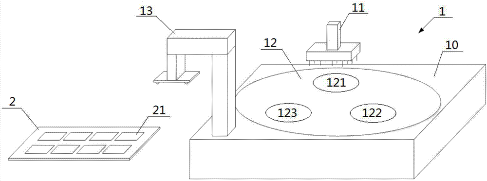
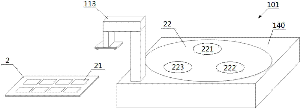
[0026] In the first embodiment, the PCB automatic test system 101 without carry waiting time of the present invention is as figure 1 As shown, a test bench 140 and a robot arm 113 are included, and the test bench 140 has a station 22 on it. Eight single-piece PCB boards 2 such as single-piece 21 are grasped and placed on the station 22 of the test bench 110 by the mechanical arm 113 of the PCB automatic test system 101 without carry waiting time of the present invention to accept different tests.

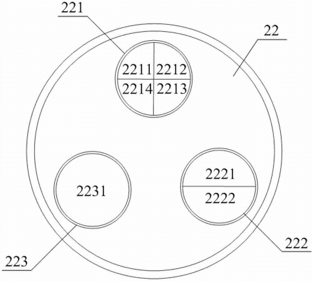
[0027] image 3 show figure 2 Shown in station 22. Station 22 is a rotating disk-shaped station that rotates about its central axis. There are three rotatable disc-shaped sub-stations on the station 22, which are respectively the first sub-station 221, the second sub-station 222 and the third sub-station 223, and each sub-station surrounds its respective The central axis rotates. Wherein, the test of the first sub-station 221 is a bending process, and the test time of the firs...


PUM


Abstract

The invention discloses an entrance waiting time-free automatic test system for a printed circuit board (PCB). The system comprises a mechanical arm and a test bench. A rotatable station is arranged on the test bench. A plurality of rotatable sub-stations are arranged on the station. One or more working areas are arranged on each sub-station. A test device for sub-station test is arranged on each working area of each sub-station, and rotates synchronously with the corresponding sub-station. The number of the working areas on each sub-station is directly proportional to the test time of the sub-station. When the system is used, the PCB is sequentially transmitted to each sub-station to be tested on the sub-stations by rotating the station, and is sequentially transmitted to each working area by rotating the sub-stations. The working areas in a number which is directly proportional to the test time of each sub-station are arranged on the sub-station to eliminate entrance waiting time between the sub-stations, so that the test time of the PCB is saved, and the test efficiency of the PCB is improved.

Description

technical field [0001] The invention relates to a PCB testing system, in particular to a PCB automatic testing system without carry waiting time. Background technique [0002] PCB (Printed Circuit Board) is a printed circuit board, referred to as a printed board, and is one of the important components of the electronics industry. Almost every kind of electronic equipment, ranging from electronic watches and calculators to computers, communication electronic equipment, and military weapon systems, as long as there are electronic components such as integrated circuits, printed boards are used for the electrical interconnection between them. . At present, a single PCB often includes multiple monoliths (units), and these monoliths have the same structure and pattern, so that they can be divided into multiple monoliths after the PCB board is manufactured and tested, so as to achieve large-scale Production. [0003] In the production process of PCB boards, in order to verify th...

Claims


Application Information

Patent Timeline
Patent Type & Authority Applications(China)
IPC IPC(8): G01R31/28G01R31/02G01N21/88
Inventor 顾岗郑谦陈龙郭剑锋
Owner SHANGHAI JINDONGTANG TECH CO LTD
Why Eureka
Try Eureka