A Method of Eliminating Sidelobe Graphics

A pattern and side lobe technology, applied in the field of integrated circuit manufacturing, can solve problems such as circuit failure, lack of surface inhibitors, affecting semiconductor production yield, etc., to avoid circuit failure, ensure accuracy, and improve output yield.

Active Publication Date: 2017-03-15
SHANGHAI INTEGRATED CIRCUIT RES & DEV CENT
View PDF5 Cites 0 Cited by
  • Summary
  • Abstract
  • Description
  • Claims
  • Application Information

AI Technical Summary

Problems solved by technology

Especially for 193nm lithography, due to the lack of sufficient surface inhibitors in current photosensitive materials to prevent the generation of side lobe patterns
The side lobe pattern will cause circuit failure and greatly affect the yield of semiconductor production

Method used


Image

  • A Method of Eliminating Sidelobe Graphics
  • A Method of Eliminating Sidelobe Graphics
  • A Method of Eliminating Sidelobe Graphics

Examples


Embodiment Construction

[0027] A method for eliminating side lobe patterns provided by the present invention will be described in further detail below in conjunction with the accompanying drawings and specific embodiments. Advantages and features of the present invention will be apparent from the following description and claims. It should be noted that all the drawings are in a very simplified form and use imprecise scales, and are only used to facilitate and clearly assist the purpose of illustrating the embodiments of the present invention.

[0028] now attached Figure 2-10 , a method for eliminating sidelobe patterns of the present invention is further described in detail through a specific embodiment. It should be noted that all the drawings are in a very simplified form and use imprecise scales, and are only used to facilitate and clearly assist the purpose of illustrating the embodiments of the present invention.

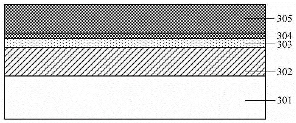
[0029] figure 2 It is a schematic diagram of the preparation process of a ...


PUM

PropertyMeasurementUnit
transmittivityaaaaaaaaaa

Abstract

The invention provides a method for eliminating a side lobe pattern. The method comprises the following steps of: providing a substrate, and forming a target material layer, a hard mask layer, a first bottom anti-reflection layer and a first photoresist on the substrate in sequence; exposing, performing photo-etching, and defining a side lobe pattern area on the hard mask layer by using a first mask pattern; coating a second bottom anti-reflection layer and a second photoresist on the hard mask layer in sequence; exposing, and forming a target pattern and a side lobe pattern in the second photoresist by using a second mask pattern; etching, defining a pattern of the target material layer by using a target pattern in the second photoresist, and blocking the side lobe pattern in the second photoresist through the side lobe pattern area of the hard mask layer; and removing the hard mask layer. Due to the adoption of the method, the side lobe pattern is effectively blocked on the hard mask layer, the side lobe pattern is eliminated from the pattern of the target material layer, the accuracy of a patterning process is ensured, circuit failures caused by the side lobe pattern are avoided, and the yield is further increased.

Description

technical field [0001] The invention relates to the technical field of integrated circuit manufacturing, in particular to a method for eliminating side lobe graphics. Background technique [0002] With the continuous advancement of the semiconductor industry to deep submicron technology, due to the continuous reduction of the focal depth of lithography, the difficulty of designing lithography projection systems, and the complexity of manufacturing, the existing lithography technology has reached the maximum resolution limit. As a result, a series of lithographic resolution enhancement technologies emerged. [0003] Phase-shift mask is a resolution enhancement technology that has been widely used. Compared with traditional binary mask, phase-shift mask enables lithography exposure tolerance and pattern resolution to be improved. The attenuation phase shift mask replaces the opaque part of the binary mask with a partially transparent material, and the phase shifts 180 degrees...

Claims


Application Information

Patent Timeline
Patent Type & Authority Patents(China)
IPC IPC(8): H01L21/027G03F7/00
Inventor 胡红梅
Owner SHANGHAI INTEGRATED CIRCUIT RES & DEV CENT
Why Eureka
Try Eureka