LDMOS (Laterally Diffused Metal Oxide Semiconductor) transistor and manufacturing method thereof

A technology of transistors and semiconductors, which is applied in semiconductor/solid-state device manufacturing, semiconductor devices, electrical components, etc., can solve the problems of not being able to increase the breakdown voltage of LDMOS transistors, reduce the breakdown voltage of LDMOS transistors, etc., so as to improve the breakdown voltage, The effect of reducing complexity

Inactive Publication Date: 2013-04-17
SEMICON MFG INT (SHANGHAI) CORP
View PDF5 Cites 10 Cited by
  • Summary
  • Abstract
  • Description
  • Claims
  • Application Information

AI Technical Summary

Problems solved by technology

However, in the actual production process, it will be found that such an approach cannot increase the breakdown voltage of the LDMOS transistor, and even in some cases such an approach will reduce the breakdown voltage of the LDMOS transistor.

Method used


Image

  • LDMOS (Laterally Diffused Metal Oxide Semiconductor) transistor and manufacturing method thereof
  • LDMOS (Laterally Diffused Metal Oxide Semiconductor) transistor and manufacturing method thereof
  • LDMOS (Laterally Diffused Metal Oxide Semiconductor) transistor and manufacturing method thereof

Examples


Embodiment Construction

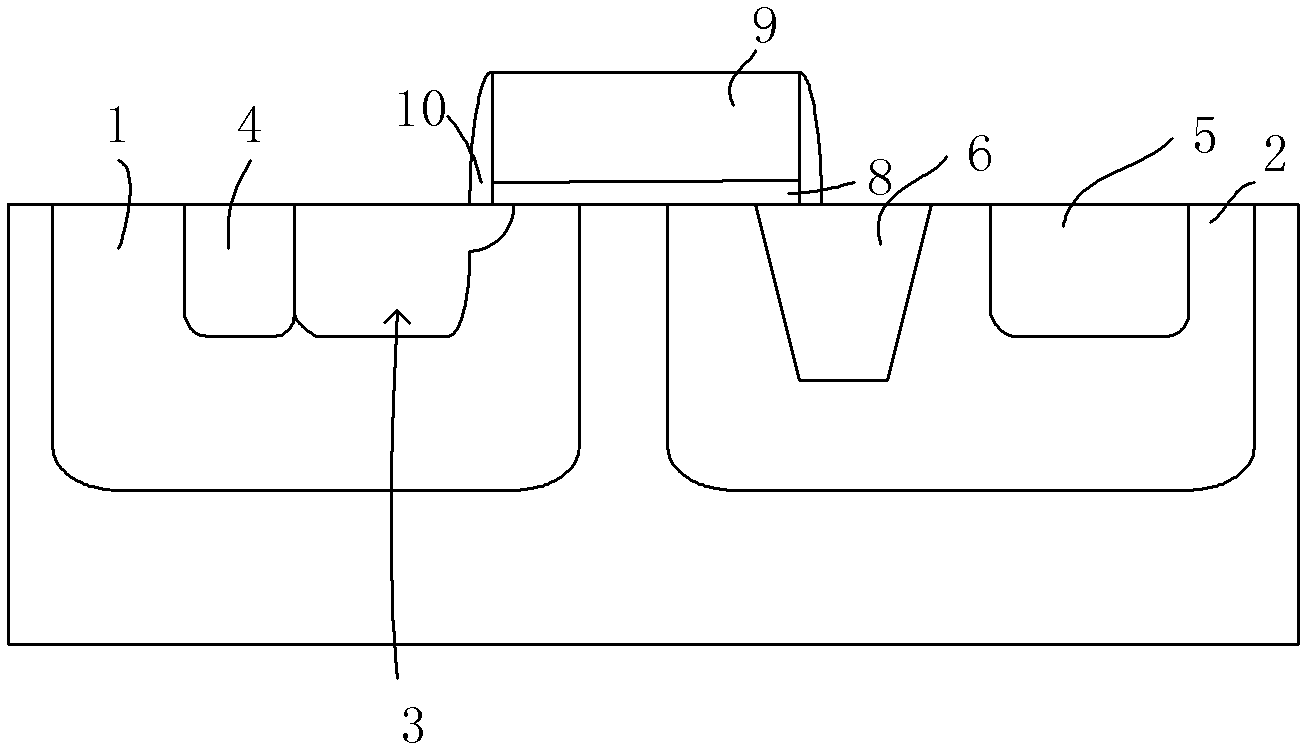
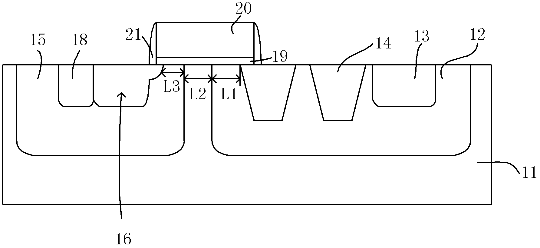
[0039] In order to increase the breakdown voltage of the LDMOS transistor, one of the methods that those skilled in the art can think of is to increase the width of the STI structure between the source region and the drain region of the transistor, but it will be found that this method does not The purpose of increasing the breakdown voltage of the transistor cannot be achieved. On the contrary, in some cases this practice even lowers the breakdown voltage of the transistor. Therefore, technicians have to improve the breakdown voltage of the LDMOS transistor from other perspectives, such as replacing the material filling the STI structure and increasing the overall size of the device.

[0040] The inventor found in practice that the reason for this phenomenon (increasing the width of the STI structure between the transistor source region and the drain region cannot increase the breakdown voltage of the transistor) is that the shallow trenches in the STI structure are etched by...


PUM


Abstract

The invention provides an LDMOS (Laterally Diffused Metal Oxide Semiconductor) transistor and a manufacturing method thereof. A plurality of STI (Shallow Trench Isolation) structures are arranged between a source region and a drain region, so that the breakdown voltage of the transistor is improved, and the problem that the central region of the bottom of the STI structure protrudes when the width of the STI structure broadens; based on the existing manufacturing process of the LDMOS transistor, the additional manufacturing process of the LDMOS transistor provided by the invention is not added, so that the degree of complexity of manufacturing is reduced; after the plurality of STI structures are formed, the subsequent manufacturing process does not need to be changed, so that the possibility of impact on certain characteristics of other devices positioned on the same semiconductor substrate is avoided; and the impact on some characteristics of the transistor itself is also avoided.

Description

technical field [0001] The invention relates to the field of double diffused metal oxide semiconductors (DMOS), in particular to an LDOMS transistor and a manufacturing method thereof. Background technique [0002] In power applications, since DMOS (double-diffused metal-oxide-semiconductor) technology adopts a vertical device structure (such as a vertical NPN bipolar transistor), it has many advantages, including high current drive capability, low on-resistance and high breakdown Voltage, etc., the document of patent No. 200810103337 discloses a high voltage resistant DMOS transistor. There are two main types of DMOS transistors, vertical double-diffused metal oxide semiconductor field effect transistor VDMOSFET (vertical double-diffused MOSFET) and lateral double-diffused metal oxide semiconductor field effect transistor LDMOSFET (lateral double-dif fused MOSFET). Compared with common field effect transistors, LDMOS transistors have obvious advantages in key device charac...

Claims


Application Information

Patent Timeline
Patent Type & Authority Applications(China)
IPC IPC(8): H01L29/78H01L21/762H01L21/336
Inventor 曹国豪郑大燮
Owner SEMICON MFG INT (SHANGHAI) CORP
Why Eureka
Try Eureka