Method of inspecting memory cell
A detection method and memory cell technology, which are used in semiconductor/solid-state device testing/measurement, static memory, instruments, etc., can solve the problems of increasing manufacturing costs and inability to detect memory cells in real time.
- Summary
- Abstract
- Description
- Claims
- Application Information
AI Technical Summary
Problems solved by technology
Method used
Image

Examples
Embodiment Construction
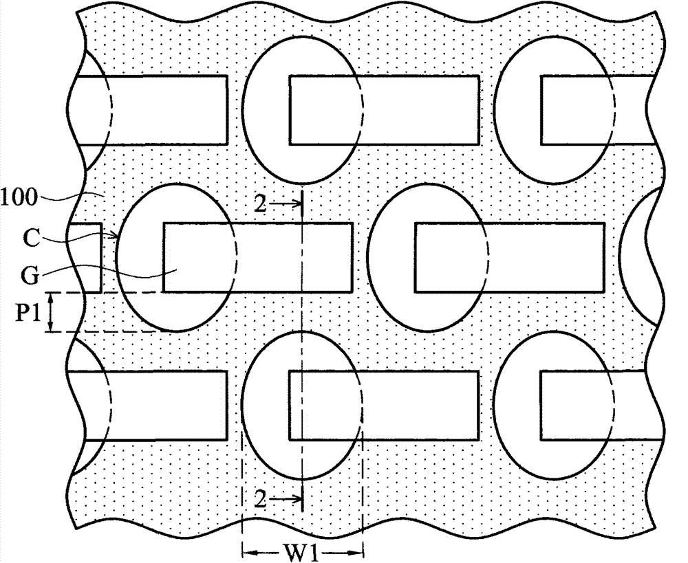
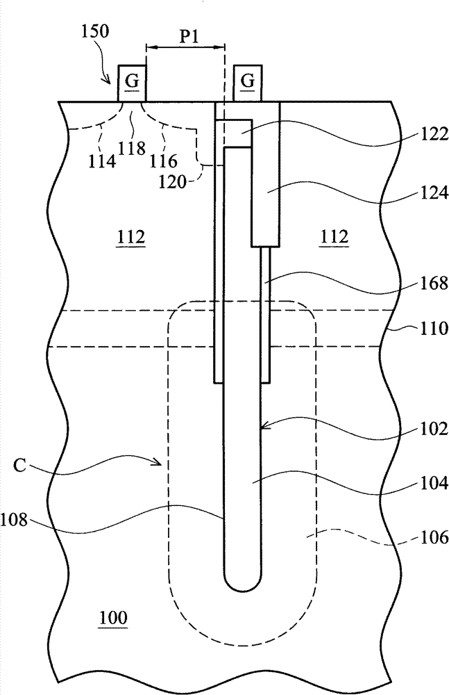
[0033] figure 1 It is a schematic top view showing the layout of the memory cell array in the DRAM device according to an embodiment of the present invention. Such as figure 1 As shown, the layout of the memory cell array here includes several capacitors C and several gate stacks G regularly arranged in and on the semiconductor substrate 100 . These capacitors C may be deep trench capacitors (deep trench capacitors) formed in the semiconductor substrate 100, and these gate stacks belong to several transistors 150 (see figure 2 ), which is formed on the top surface of the semiconductor substrate 100 and partially covers the top surfaces of the adjacent capacitors C. At this time, the entire top surfaces of the gate stacks G and part of the top surfaces of the capacitors C are exposed, and no additional film layer is formed thereon.
[0034] figure 2 for along figure 1 The cross-section of the inner line 2-2 shows these capacitors C and the two gate stacks G formed on and...
PUM
 Abstract
Description
Claims
Application Information
 - Generate Ideas
- Intellectual Property
- Life Sciences
- Materials
- Tech Scout
- Unparalleled Data Quality
- Higher Quality Content
- 60% Fewer Hallucinations
Browse by: Latest US Patents, China's latest patents, Technical Efficacy Thesaurus, Application Domain, Technology Topic, Popular Technical Reports.
© 2025 PatSnap. All rights reserved.Legal|Privacy policy|Modern Slavery Act Transparency Statement|Sitemap|About US| Contact US: help@patsnap.com