A method for preparing a gate dielectric structure using ald

A technology of gate dielectric and equipment, applied in semiconductor/solid-state device manufacturing, semiconductor devices, electrical components, etc., can solve the problems of insufficiency of devices, large gate leakage current, etc., and achieve the effect of uniform distribution and improved electrical performance

Active Publication Date: 2015-11-18
INST OF MICROELECTRONICS CHINESE ACAD OF SCI
View PDF5 Cites 0 Cited by
  • Summary
  • Abstract
  • Description
  • Claims
  • Application Information

AI Technical Summary

Problems solved by technology

In terms of device performance, considerable literature has studied Al 2 o 3 / HfO 2 When stacked layers are used as the gate dielectric, its dielectric constant is relatively high, and there is no voltage hysteresis, and the breakdown voltage of the device is also high, but its gate leakage current at low voltage is very large, which cannot meet the requirements of the device.

Method used


Image

  • A method for preparing a gate dielectric structure using ald
  • A method for preparing a gate dielectric structure using ald
  • A method for preparing a gate dielectric structure using ald

Examples


Embodiment Construction

[0032] The principles and features of the present invention are described below in conjunction with the accompanying drawings, and the examples given are only used to explain the present invention, and are not intended to limit the scope of the present invention.

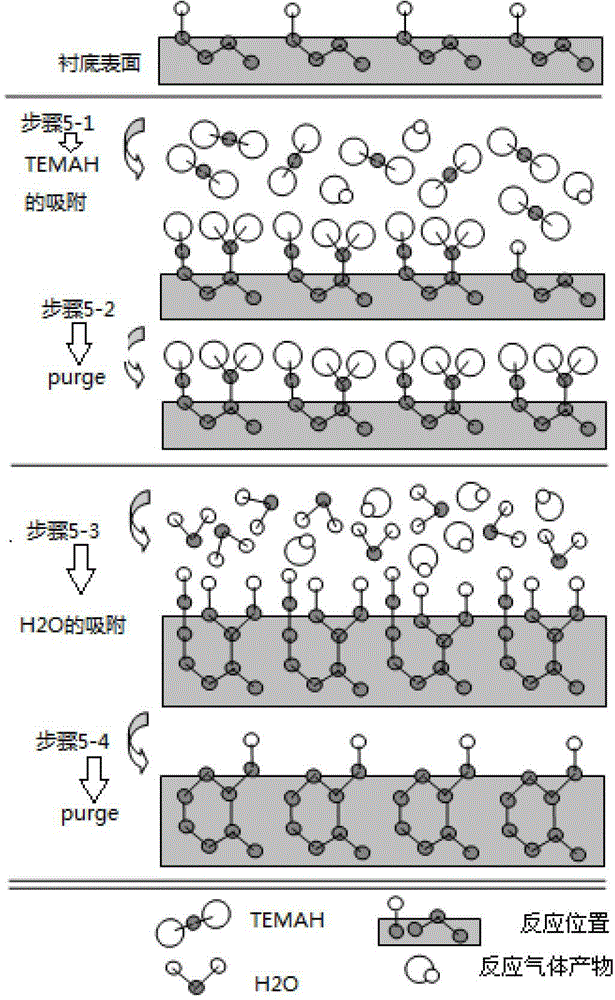
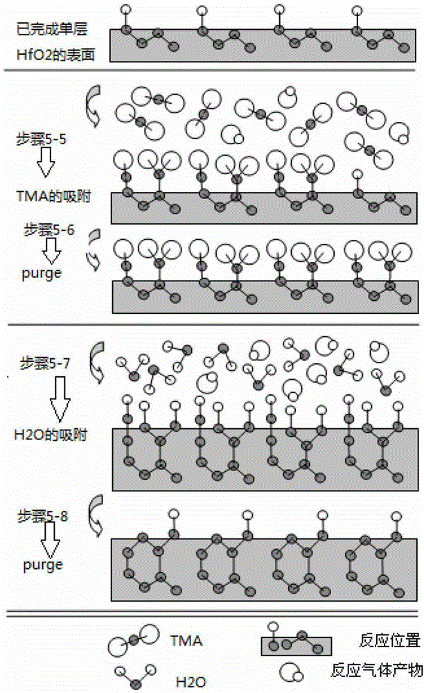
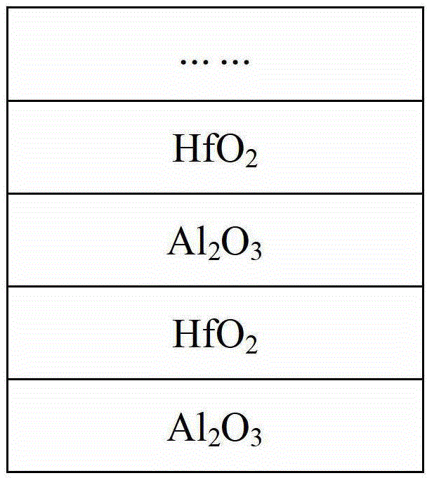
[0033] An embodiment of the present invention provides a method for preparing a gate dielectric structure using ALD, including the following steps:

[0034] Step 101, perform standard RCA cleaning on the substrate, using H 2 SO 4 :H 2 o 2 =5:100 Boil for 5 minutes; then rinse with deionized water (DIwater); then use HF:H 2 O=5:95 Soak for 2 minutes; use N at the end 2 blow dry;

[0035] Step 102, put the substrate into the chamber of the ALD equipment; vacuumize the chamber, and at the same time heat the peripheral parts of the ALD equipment that need to be heated; after the vacuum of the chamber is pumped below 1torr, the substrate is heating;

[0036] Step 103, through the carrier gas N 2 The tetramethylet...


PUM


Abstract

A method for preparing a gate dielectric structure by ALD comprises the following steps: step (1), placing a substrate in a chamber of an ALD apparatus; step (2), growing a monolayer of HfO2 on the surface of the substrate; step (3), growing a monolayer of Al2O3 on the surface of the monolayer of HfO2; step (4), repeating the step (2) and the step (3), and obtaining the gate dielectric structure with alternately grown HfO2 and Al2O3. The gate dielectric structure with alternately grown HfO2 and Al2O3 prepared in the present invention can sufficiently achieve atom combination and interaction of Hf and Al, and improve electrical performance of the gate dielectric.

Description

technical field [0001] The invention relates to the technical field of preparing integrated circuit devices, in particular to a method for preparing a gate dielectric structure by using ALD. Background technique [0002] With the rapid development of integrated circuit technology, the feature size of MOS field effect transistors continues to shrink, SiO 2 As a gate dielectric material, it can no longer meet the needs of the development of integrated circuit technology below 45nm, and use high-k gate dielectric to replace SiO 2 The gate dielectric can increase the physical thickness of the dielectric layer under the condition of keeping the equivalent oxide layer unchanged, thereby effectively reducing the gate leakage. [0003] HfO 2 As a recently researched gate dielectric material, it has a high dielectric constant (relative dielectric constant is about 25), stable chemical properties and sufficient energy band difference. Experiments have shown that when using HfO 2 W...

Claims


Application Information

Patent Timeline
Patent Type & Authority Patents(China)
IPC IPC(8): H01L21/285
CPCH01L29/517H01L21/02178H01L21/02181H01L21/022H01L21/0228H01L21/28194
Inventor 董亚斌夏洋李超波张阳
Owner INST OF MICROELECTRONICS CHINESE ACAD OF SCI
Why Eureka
Try Eureka