Low-differential-pressure voltage stabilizer circuit with auxiliary circuit
A low-dropout voltage regulator and auxiliary circuit technology, which is applied in the direction of instruments, electric variable adjustment, control/regulation systems, etc., can solve problems such as easy breakdown, device failure, and large overshoot voltage
- Summary
- Abstract
- Description
- Claims
- Application Information
AI Technical Summary
Problems solved by technology
Method used
Image

Examples
Embodiment Construction
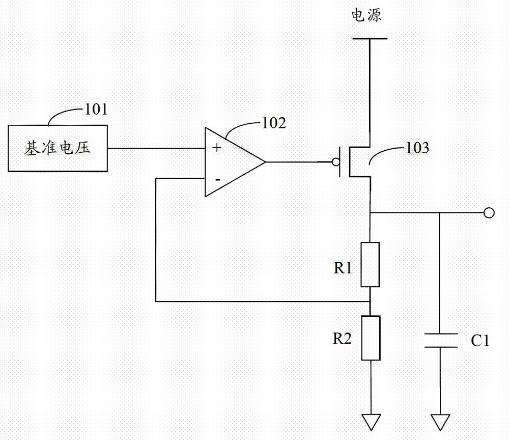
[0030] It can be seen from the background technology that low dropout voltage regulators are usually used in electronic equipment to provide stable working voltage for the working circuit, but the state of the working circuit changes, especially when the working circuit of the digital circuit changes from the on state to the off state. In the case of a sudden drop in load current, the output voltage signal of the low dropout voltage regulator will produce a large overshoot. Although the existing technology can reduce the voltage overshoot by setting a decoupling capacitor at the output end of the low dropout voltage regulator, However, due to cost considerations, the decoupling capacitors described above are usually small and the effect is not good.
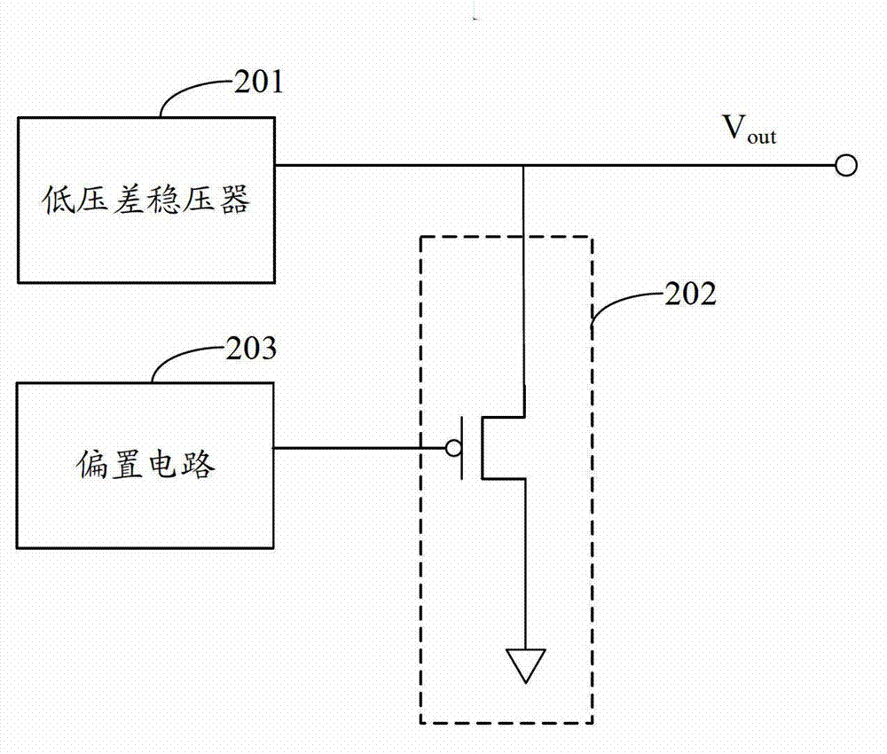
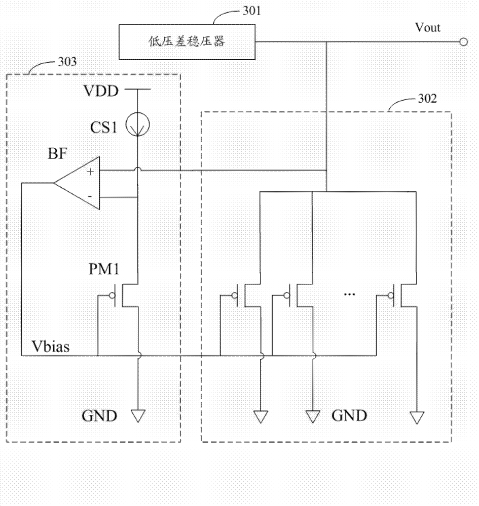
[0031] For this reason, the present invention provides a kind of low dropout regulator circuit with auxiliary circuit, please refer to figure 2 , the low dropout voltage regulator circuit with auxiliary circuit includes: low dro...
PUM
 Abstract
Description
Claims
Application Information