Data writing and reading methods and devices

A technology for data writing and data reading, applied in the computer field

Inactive Publication Date: 2013-05-01
HUAWEI TECH CO LTD
View PDF3 Cites 25 Cited by
  • Summary
  • Abstract
  • Description
  • Claims
  • Application Information

AI Technical Summary

Problems solved by technology

[0004] When a bus interface performs read and write access to a memory, other bus interfaces that need to access the memory need to wait. Therefore, the read and write access efficiency of the bus interface to the memory directly affects the delay time of the read and write operations. This delay is especially noticeable when the same memory reads and writes a large amount of data continuously

Method used


Image

  • Data writing and reading methods and devices
  • Data writing and reading methods and devices
  • Data writing and reading methods and devices

Examples


Embodiment Construction

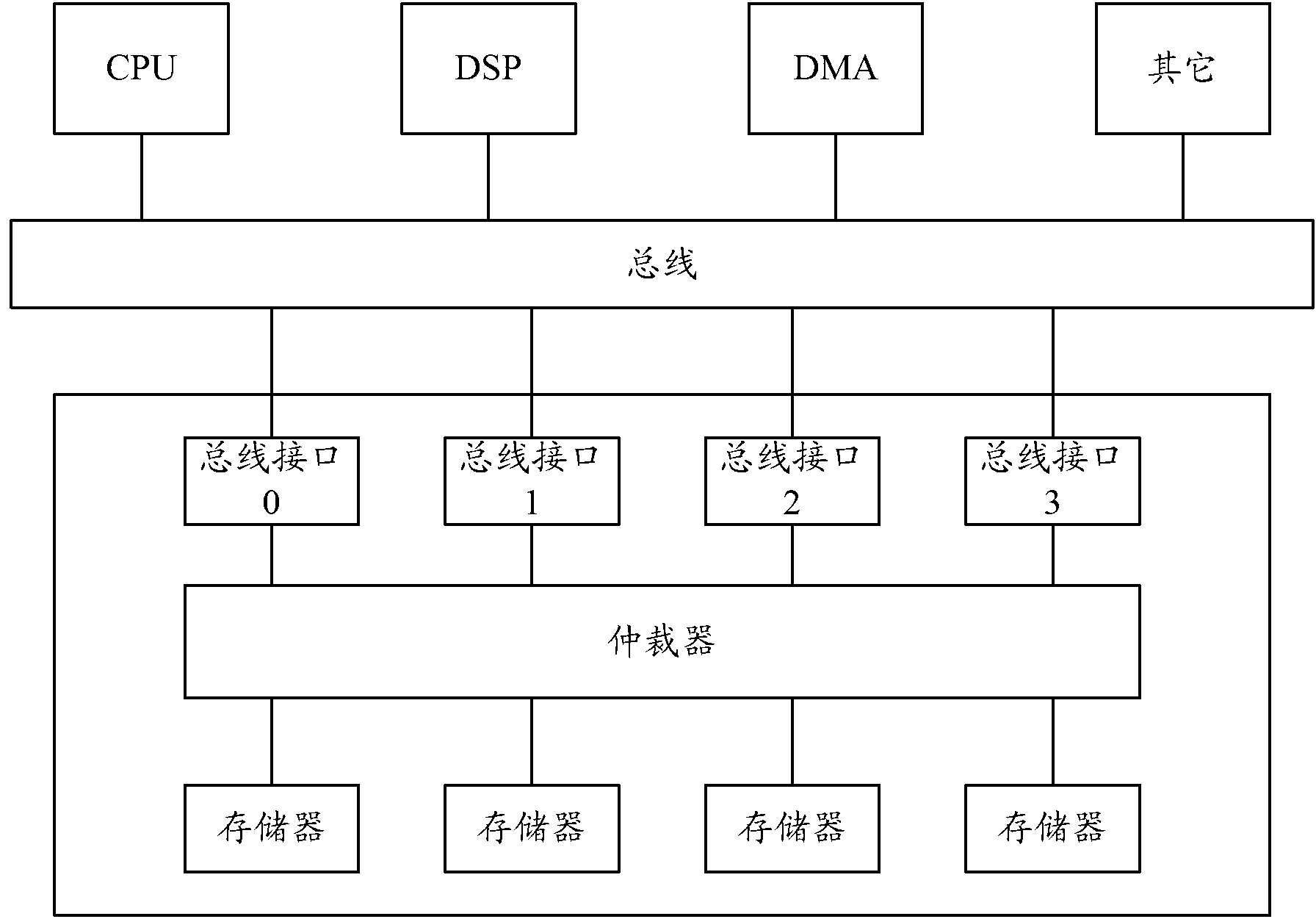
[0080] figure 1 It is a schematic diagram of a typical application scenario of the data writing and reading method of the embodiment of the present invention. Such as figure 1 As shown, multiple bus interfaces are integrated on the shared memory controller. After receiving the read and write requests from the CPU, DSP, Direct Memory Access (DMA) or any other modules on the bus, the bus interface passes The arbiter performs read or write operations on the corresponding memory. The data writing and reading method of the embodiment of the present invention is for example by figure 1 implemented via the integrated bus interface on the shared memory controller. below to apply to figure 1 In the shown scene, the data writing and reading method of the embodiment of the present invention will be described in detail.

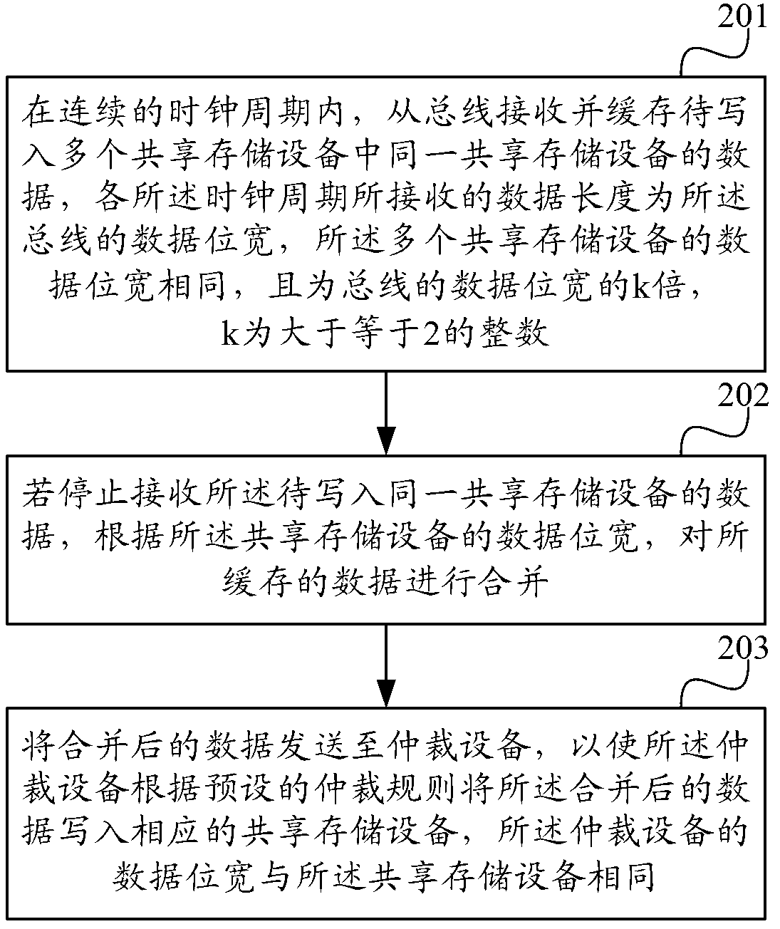
[0081] figure 2 It is a schematic flowchart of a data writing method according to an embodiment of the present invention. Such as figure 2 As shown, the data w...


PUM


Abstract

The embodiment of the invention provides a data writing method, a data writing device, a data reading method and a data reading device. The data writing method comprises the following steps of: in continuous clock cycles, receiving data to be written into the same shared memory equipment in a plurality of pieces of shared memory equipment from a bus, and caching the data, wherein the length of the data received in each clock cycle is the data bit width of the bus, the data bit widths of the pieces of shared memory equipment are the same, and are k times that of the bus, and k is an integer more than or equal to 2; if the reception of the data to be written into the same shared memory equipment is stopped, merging the cached data according to the data bit width of the shared memory equipment; and transmitting the merged data to arbitration equipment, so that the arbitration equipment writes the merged data into the corresponding shared memory equipment according to preset arbitration rules, wherein the data bit width of the arbitration equipment is the same as that of the shared memory equipment.

Description

technical field [0001] The invention relates to data processing technology, in particular to a data writing and reading method and device, and belongs to the field of computer technology. Background technique [0002] With the development of design and manufacturing technology, a system-on-chip (System On Chip, SOC) that can effectively reduce the development cost of electronic products and shorten the development cycle has emerged. The SoC integrates a central processing unit (Central Processing Unit, CPU), a data signal processing (Digital Signal Processing, DSP) core, memory, and other dedicated functional logic modules. Among them, the time-sensitive shared data between CPU, DSP core and other special function logic modules is often stored in the internal memory (Memory). [0003] SOC also usually includes a shared memory controller, which includes a plurality of bus interfaces connected to the bus, for receiving read and write accesses transmitted by the CPU, DSP core,...

Claims


Application Information

Patent Timeline
Patent Type & Authority Applications(China)
IPC IPC(8): G06F12/02
Inventor 朱建华
Owner HUAWEI TECH CO LTD
Why Eureka
Try Eureka