Back collector structure of power semiconductor devices

A power semiconductor and collector technology, applied in semiconductor devices, circuits, electrical components, etc., can solve the problems of complex reliability of back gold process, mismatch of heterogeneous materials lattice, and greater impact on device performance than the original process. Achieve the effect of improving turn-off characteristics, improving on-state voltage drop, and reducing carrier lifetime

Active Publication Date: 2015-08-12
JIANGSU R & D CENTER FOR INTERNET OF THINGS +2
View PDF4 Cites 0 Cited by
  • Summary
  • Abstract
  • Description
  • Claims
  • Application Information

AI Technical Summary

Problems solved by technology

[0004] Due to the lattice mismatch of heterogeneous materials, the growth is prone to defects, and poor technical control will have a great impact on the performance of the device
The follow-up ohmic contact problem caused by new materials is immature compared with the existing Si process, which may cause the back gold process to be more complicated than the original process or cause reliability problems

Method used


Image

  • Back collector structure of power semiconductor devices
  • Back collector structure of power semiconductor devices
  • Back collector structure of power semiconductor devices

Examples


Embodiment 1

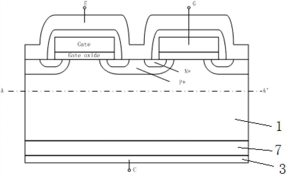
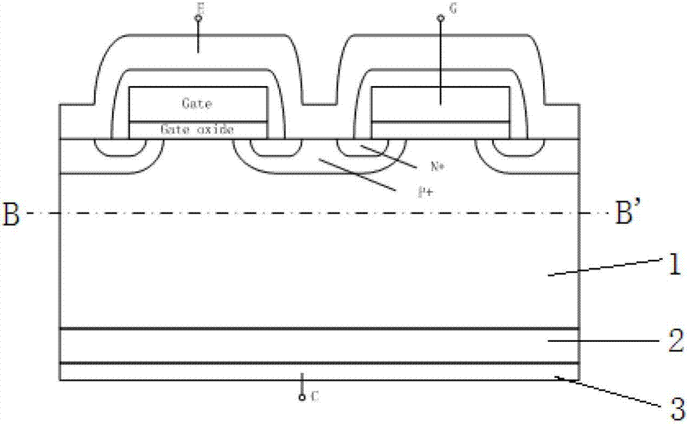
[0025] Such as figure 2 As shown in the back collector structure of the power semiconductor device, a P conductivity type gallium nitride layer 2 is provided on the back surface of the N conductivity type silicon substrate 1 , and a collector electrode 3 is provided on the back surface of the P conductivity type gallium nitride layer 2 .

[0026] figure 2 The area above the middle BB' line is the front structure of the power semiconductor device, which is related to figure 1 The front structures of the power semiconductor devices in the region above the middle AA' line are exactly the same. This embodiment is similar to Embodiment 1, and it replaces the P conductivity type silicon collector layer 7 in Embodiment 1 with the P conductivity type gallium nitride layer 2 .

[0027] The P-conductivity-type gallium nitride layer 2 material on the back is prepared by epitaxy. Since the doping concentration of the P-conductivity-type gallium nitride layer 2 cannot be too high, the ...

Embodiment 2

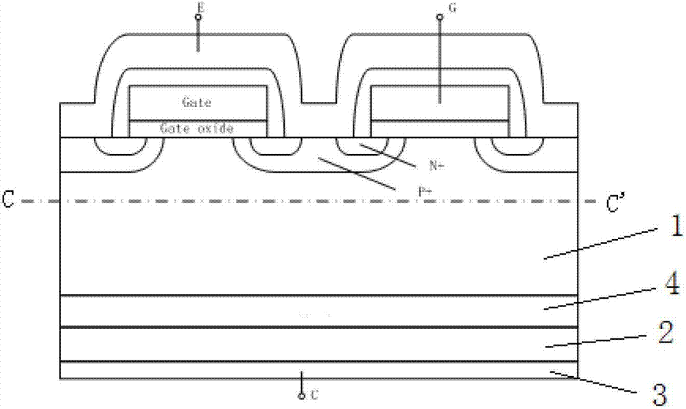
[0032] Such as image 3 As shown in the back collector structure of the power semiconductor device, a P conductivity type gallium nitride layer 2 is provided on the back surface of the N conductivity type silicon substrate 1, and a collector electrode 3 is provided on the back surface of the P conductivity type gallium nitride layer 2. A first buffer layer 4 is provided between the N conductive type silicon substrate 1 and the P conductive type gallium nitride layer 2 , and the first buffer layer 4 is an N conductive type silicon buffer layer.

[0033] image 3 The area above the middle CC' line is the front structure of the power semiconductor device, which is related to figure 1 The front structures of the power semiconductor devices in the region above the middle AA' line are exactly the same. This embodiment is similar to Embodiment 1, a first buffer layer 4 is added between the N conductivity type silicon substrate 1 and the P conductivity type gallium nitride layer 2, ...

Embodiment 3

[0035] Such as Figure 4 As shown in the back collector structure of the power semiconductor device, a P conductivity type gallium nitride layer 2 is provided on the back surface of the N conductivity type silicon substrate 1, and a collector electrode 3 is provided on the back surface of the P conductivity type gallium nitride layer 2. Between the N conductive type silicon substrate 1 and the P conductive type gallium nitride layer 2, a first buffer layer 4 is provided, and the first buffer layer 4 is an N conductive type silicon buffer layer, and between the first buffer layer 4 and the P A second buffer layer 5 is arranged between the conductive type gallium nitride layer 2, and the second buffer layer 5 is an amorphous gallium nitride layer or an aluminum nitride buffer layer; between the P conductive type gallium nitride layer 2 and the collector 3 is provided with an indium gallium nitride layer 6 .

[0036] Figure 4 The front structure of the medium-power semiconduct...


PUM


Abstract

The invention relates to a backside collector structure of a power semiconductor device. According to the technical scheme provided by the invention, in the backside collector structure of the power semiconductor device, a P conductive-type gallium-nitride layer is arranged on the backside of an N conductive-type silicon substrate, and a collector is arranged on the backside of the P conductive-type gallium-nitride layer. According to the invention, a heterojunction structure is manufactured on the backside of the device, so that the injection efficiency is improved, and the conducting voltage drop of the device can be improved; and a heterojunction interface has more defects, so that a recombination center can be formed, and therefore, the service life of current carriers is reduced, and turn-off characteristics are improved.

Description

technical field [0001] The invention relates to the technical field of power semiconductor devices, in particular to a back collector structure of a power semiconductor device. Background technique [0002] Chinese patent application number: 201010554510.5, in the process of LED epitaxial growth, GaN material is deposited. Next, after the LED epitaxial growth is completed, the transparent electrode layer is deposited. Then, the deposited transparent electrode layer is made into a grid-like layer. Through the existence of the grid-shaped high dielectric constant transparent electrode layer, it can be used as a current spreading layer and a stress buffering layer. [0003] Patent application number: 200480038612.4, providing a semiconductor device with a heterojunction. The device includes a substrate and at least one nanostructure. Substrates and nanostructures are composed of different materials. The substrate can be composed of, for example, a group IV semiconductor ma...

Claims


Application Information

Patent Timeline
Patent Type & Authority Patents(China)
IPC IPC(8): H01L29/417
Inventor 陈宏朱阳军邱颖斌徐承福吴凯
Owner JIANGSU R & D CENTER FOR INTERNET OF THINGS
Why Eureka
Try Eureka