Process optimization method of carrier storage trench gate bipolar transistor structure

A bipolar transistor and carrier storage technology, which is applied in the direction of semiconductor devices, semiconductor/solid-state device manufacturing, electrical components, etc., can solve the problems of low efficiency, CSTBT conduction loss and safety operating area and other performance degradation problems, to achieve The effect of increasing the concentration of the CS layer, reducing the depth, reducing the conduction voltage drop and saturation current

Pending Publication Date: 2022-03-11
FUDAN UNIV
View PDF0 Cites 0 Cited by
  • Summary
  • Abstract
  • Description
  • Claims
  • Application Information

AI Technical Summary

Problems solved by technology

In the existing process, the CS layer implantation is limited by the long-term high-temperature annealing process in the subsequent process, so the efficiency is low, which greatly reduces the conduction loss and safe operating area of ​​​​the CSTBT.

Method used


Image

  • Process optimization method of carrier storage trench gate bipolar transistor structure
  • Process optimization method of carrier storage trench gate bipolar transistor structure
  • Process optimization method of carrier storage trench gate bipolar transistor structure

Examples


Embodiment Construction

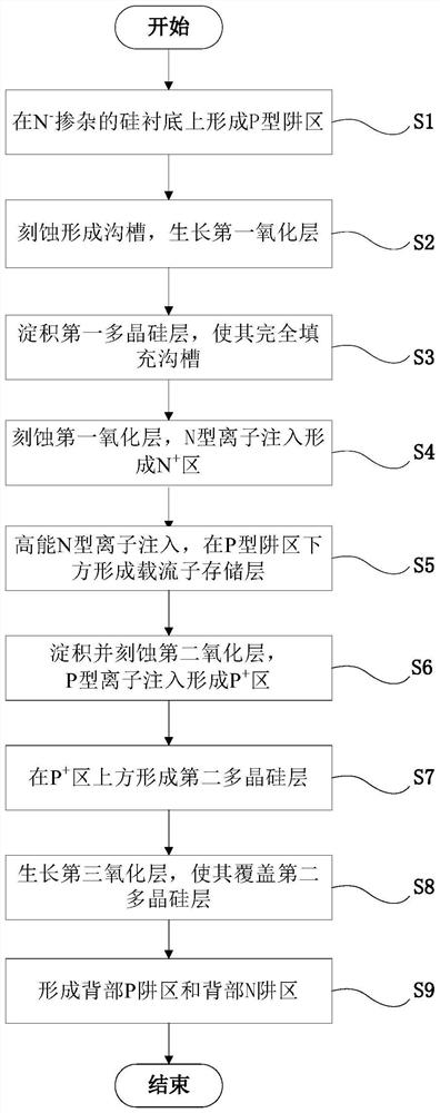
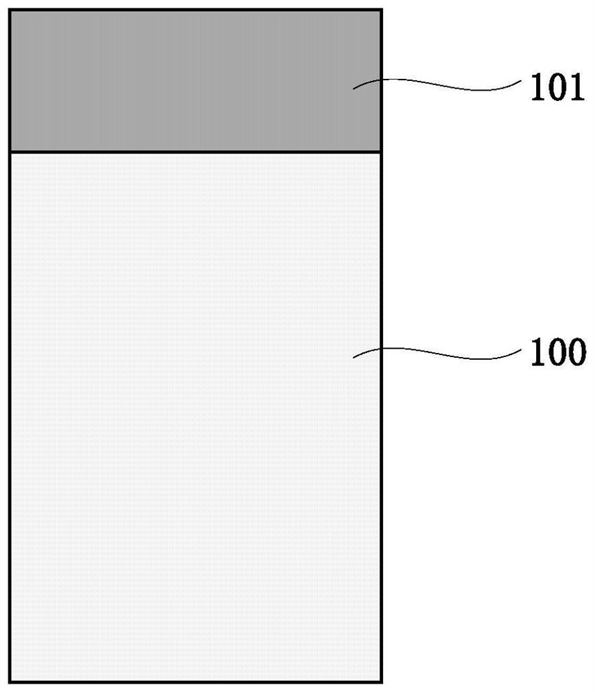
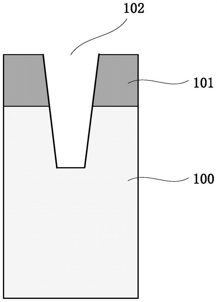
[0010] In order to make the purpose, technical solutions and advantages of the present invention clearer, the technical solutions in the embodiments of the present invention will be clearly and completely described below in conjunction with the accompanying drawings in the embodiments of the present invention. It should be understood that the specific The examples are only used to explain the present invention, not to limit the present invention. The described embodiments are only some, not all, embodiments of the present invention. Based on the embodiments of the present invention, all other embodiments obtained by persons of ordinary skill in the art without making creative efforts belong to the protection scope of the present invention.

[0011] In the description of the present invention, it should be noted that the orientation or positional relationship indicated by the terms "upper", "lower", "vertical" and "horizontal" are based on the orientation or positional relation...


PUM


Abstract

The invention discloses a process optimization method of a carrier storage trench gate bipolar transistor structure. By adjusting the injection sequence and the injection energy of the carrier storage layer, the injection efficiency of the carrier storage layer is remarkably improved, the concentration of the carrier storage layer is increased, and the conduction voltage drop and the saturation current of the carrier storage trench gate bipolar transistor are reduced.

Description

technical field [0001] The invention relates to the technical field of semiconductors, in particular to a process optimization method for a carrier storage tank gate bipolar transistor structure. Background technique [0002] Power electronic equipment is the basis for the development and progress of power electronics technology. High-performance power electronics can save electricity, thereby saving fossil energy and reducing environmental pollution. An insulated gate bipolar transistor (IGBT) is a bipolar junction transistor (BJT) controlled by a metal-oxide semiconductor field effect transistor (MOSFET), which combines the high frequency characteristics of a power MOSFET with the low turn-on voltage drop of a BJT. , featuring high input impedance and low switching loss. At present, IGBT has become the core device of energy conversion and transmission, and is the "CPU" of power electronic devices. [0003] Although the IGBT has the characteristics of handling high volta...

Claims


Application Information

Patent Timeline
Patent Type & Authority Applications(China)
IPC IPC(8): H01L21/331
CPCH01L29/66325H01L29/66348
Inventor 徐航徐大朋陈琳孙清清张卫
Owner FUDAN UNIV
Why Eureka
Try Eureka