Insulated gate bipolar transistor and manufacturing method thereof

A technology of bipolar transistor and manufacturing method, which is applied in the direction of transistor, semiconductor/solid-state device manufacturing, semiconductor device, etc., can solve the problem of increasing the turn-on voltage drop and the turn-off time, and achieves low turn-on voltage drop and turn-off time. , the effect of increasing injection efficiency and short turn-off time

Pending Publication Date: 2021-02-02
GUANGDONG MIDEA WHITE HOME APPLIANCE TECH INNOVATION CENT CO LTD +1
View PDF0 Cites 0 Cited by
  • Summary
  • Abstract
  • Description
  • Claims
  • Application Information

AI Technical Summary

Problems solved by technology

At present, there is still no suitable method to reduce the on-voltage drop without increasing the off-time, or to reduce the off-time without increasing the on-voltage drop

Method used


Image

  • Insulated gate bipolar transistor and manufacturing method thereof
  • Insulated gate bipolar transistor and manufacturing method thereof
  • Insulated gate bipolar transistor and manufacturing method thereof

Examples


example 1

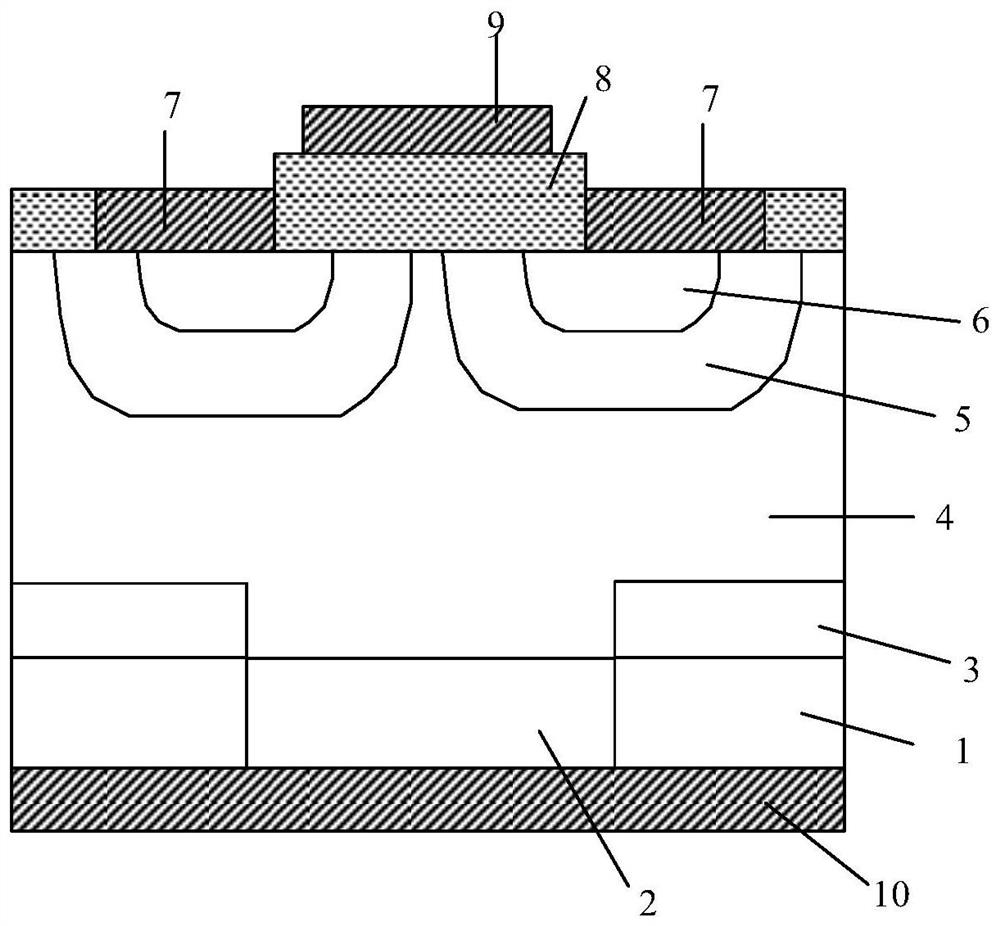
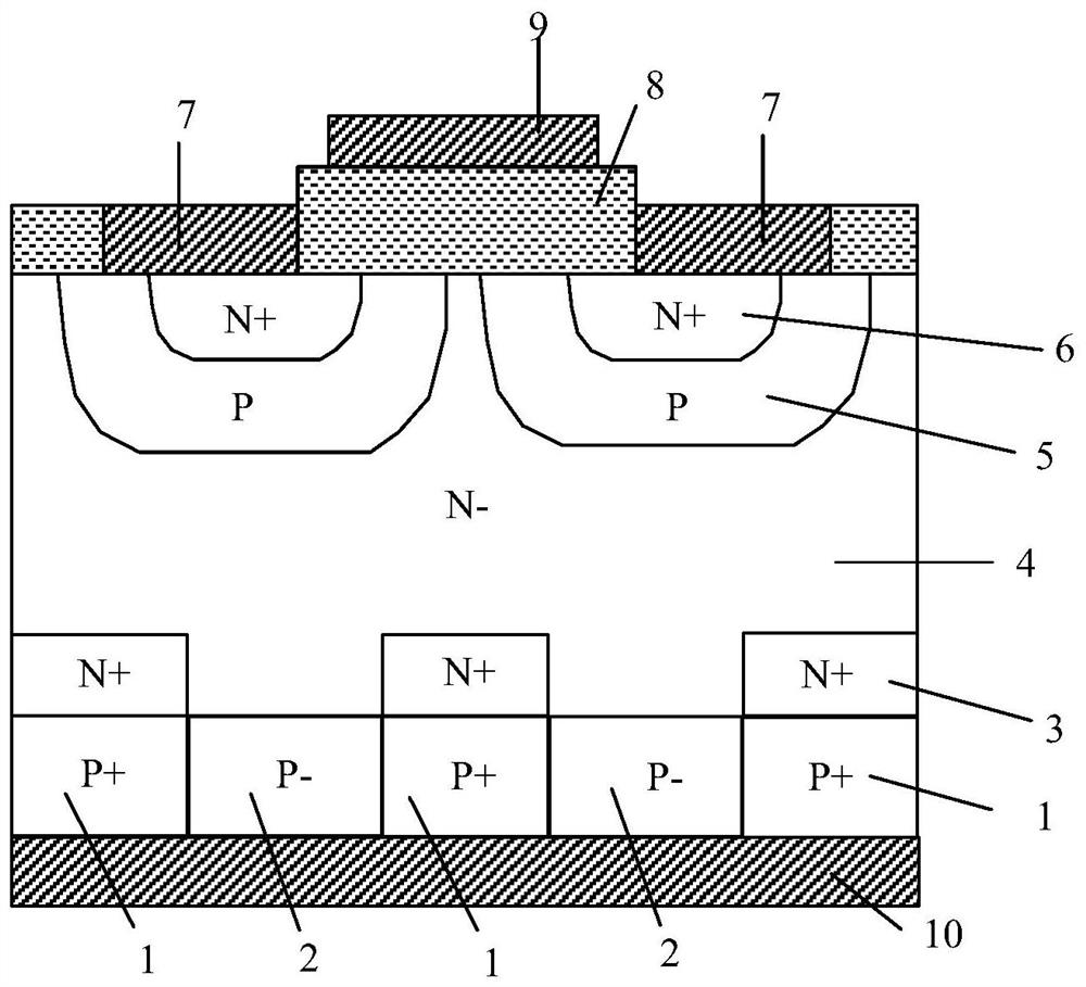
[0089] Image 6 A schematic structural diagram of an insulated gate bipolar transistor is shown. The insulated gate bipolar transistor includes: P+ collector region 1, P-collector region 2, N+ buffer layer 3, N-type drift region 4, P-type body region 5, N+ emitter region 6, emitter metal 7. Gate layer 8, gate metal 9, collector metal 10. Wherein, the doping concentration of the P+ collector region 1 is higher than that of the P− collector region 2; a positive sign (+) indicates a higher doping concentration, and a negative sign (-) indicates a lower doping concentration.

[0090] In this example, the P+ collector region 1 and the P- collector region 2 are repeatedly set in the collector region, and the N+ buffer layer 3 is formed on the corresponding P+ collector region 1; the P-collector region 2 is N- Drift Zone 4. The N+ buffer layer can effectively increase the recombination rate of holes and reduce the turn-off time, thereby reducing the turn-off loss. At the same tim...


PUM

PropertyMeasurementUnit
thicknessaaaaaaaaaa

Abstract

The embodiment of the invention discloses an insulated gate bipolar transistor and a manufacturing method thereof. The insulated gate bipolar transistor comprises a collector region, a buffer region and a drift region; the collector region comprises a first type doped region and a second type doped region; the doping concentration of the first type doped region is greater than that of the second type doped region; the buffer region is located above the first type doped region; the doping type of the buffer region is different from the doping type of the first type doped region; the drift region is located above the buffer region and the second type doped region; the doping concentration of the drift region is smaller than that of the buffer region.

Description

technical field [0001] Embodiments of the present invention relate to the technical field of semiconductors, in particular to an insulated gate bipolar transistor and a manufacturing method thereof. Background technique [0002] Insulated Gate Bipolar Transistor (IGBT for short) is a composite fully-controlled voltage-driven power semiconductor device composed of a bipolar transistor (BJT) and an insulated gate field effect transistor (MOSFET), and has a MOSFET Due to the high input impedance of the device and the low turn-on voltage drop of the power transistor (giant transistor, referred to as GTR), the drive power is small and the saturation voltage is reduced. At present, the IGBT is widely used as a new type of power electronic device. each field. [0003] The collector carrier injection efficiency and extraction efficiency of the IGBT largely determine the conduction voltage drop and switching characteristics. At present, there is still no suitable method to reduce t...

Claims


Application Information

Patent Timeline
Patent Type & Authority Applications(China)
IPC IPC(8): H01L29/739H01L21/331
CPCH01L29/7395H01L29/66333
Inventor 刘利书冯宇翔
Owner GUANGDONG MIDEA WHITE HOME APPLIANCE TECH INNOVATION CENT CO LTD
Why Eureka
Try Eureka