A kind of cstbt device and manufacturing method thereof

A device, N-type technology, applied in the field of semiconductor power devices, can solve the problems of affecting the compromise characteristics of device switching loss, increasing device switching loss, and reducing switching speed, etc.

Active Publication Date: 2020-09-15
UNIV OF ELECTRONICS SCI & TECH OF CHINA
View PDF4 Cites 0 Cited by
  • Summary
  • Abstract
  • Description
  • Claims
  • Application Information

AI Technical Summary

Problems solved by technology

[0005] The implementation of method (1) will increase the gate-emitter capacitance and gate-collector capacitance at the same time, and the switching process of the IGBT is essentially the process of charging / discharging the gate capacitance, so the increase in the gate capacitance will Makes the charging / discharging time longer, which in turn causes the switching speed to decrease
Therefore, the deep trench gate depth will reduce the switching speed of the device, increase the switching loss of the device, and affect the compromise characteristics of the device's conduction voltage drop and switching loss; and the implementation of method (2) will increase the device's switching loss The gate capacitance will reduce the switching speed of the device and increase the switching loss, which will affect the compromise between the conduction voltage drop and switching loss of the device. On the other hand, it will also increase the saturation current density of the device and make the short-circuit safe working area of ​​the device worse.
In addition, the gate oxide layer in the trench gate structure is formed in the trench by one thermal oxidation. In order to ensure a certain threshold voltage, the thickness of the entire gate oxide layer is required to be small. However, the MOS capacitance and the thickness of the oxide layer Inversely proportional, which makes the thin gate oxide thickness in traditional CSTBT devices will significantly increase the gate capacitance of the device, and the electric field concentration effect at the bottom of the trench will reduce the breakdown voltage of the device, resulting in poor reliability of the device

Method used


Image

  • A kind of cstbt device and manufacturing method thereof
  • A kind of cstbt device and manufacturing method thereof
  • A kind of cstbt device and manufacturing method thereof

Examples


Embodiment 1

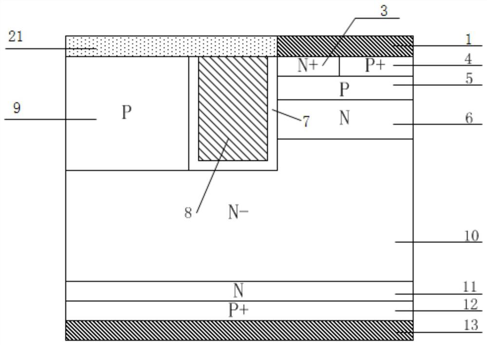
[0065] This example proposes as figure 2 A kind of CSTBT device shown, its cell structure includes: collector structure, drift region structure, emitter structure and groove gate structure; Described collector structure comprises P+ collector region 12 and is positioned at P+ collector region 12 lower surface The collector metal 13; the drift region structure includes an N-type electric field stop layer 11 and an N-type drift region layer 10 located on the upper surface of the N-type electric field stop layer 11, and the N-type electric field stop layer 11 is located in the P+ collector region 12 The upper surface of the trench gate structure; the trench gate structure is a trench gate structure, the trench gate structure penetrates into the N-type drift region 10 along the vertical direction of the device to form a trench, and the emitter structure is located on one side of the trench gate structure The emitter structure includes an emitter metal 1, an N+ emitter region 3, a...

Embodiment 2

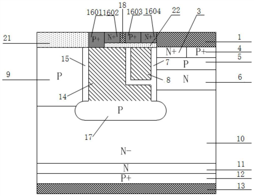
[0067] This example proposes as image 3 The shown CSTBT device has the same structure as that of Embodiment 1 except that the thickness of the trench-split electrode dielectric layer 15 is greater than that of the gate dielectric layer 7 .

[0068] Compared with Embodiment 1, this embodiment can further reduce the gate capacitance on the one hand, increase the switching speed of the device and reduce the switching loss, and on the other hand can further improve the electric field concentration effect at the bottom of the trench and increase the breakdown voltage of the device. , improve device reliability.

Embodiment 3

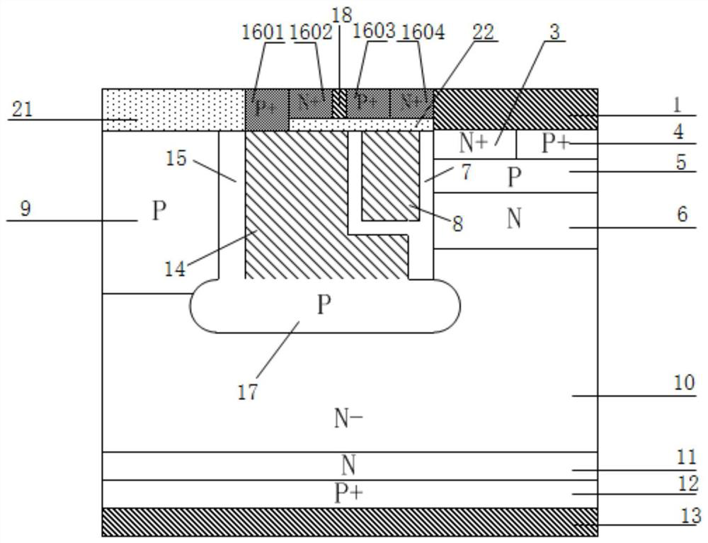
[0070] This example proposes as Figure 4 A CSTBT device shown, its cell structure includes: a collector structure, a drift region structure, an emitter structure and a groove gate structure; the collector structure includes a P+ collector region 12 and is located under the P+ collector region 12 The collector metal 13 on the surface; the drift region structure includes an N-type electric field stop layer 11 and an N-type drift region layer 10 located on the upper surface of the N-type electric field stop layer 11, and the N-type electric field stop layer 11 is located in the P+ collector region 12; the trench gate structure is a trench gate structure, the trench gate structure penetrates into the N-type drift region 10 along the vertical direction of the device to form a trench, and the emitter structure is located on both sides of the trench gate structure And connected to it; the emitter structure includes emitter metal 1, N+ emitter region 3, P+ contact region 4, P-type ba...


PUM


Abstract

A CSTBT device and a manufacturing method thereof belong to the field of semiconductor power devices. In the present invention, a trench gate structure is formed by introducing a trench split electrode under the gate electrode, a P-type layer is introduced under the trench split electrode, and a series diode structure is arranged above the trench split electrode, which solves the problem of traditional CSTBT devices by increasing the N The doping concentration of the type charge storage layer causes the problem that there is a contradictory relationship between the forward conduction performance and the withstand voltage performance of the device; the saturation current density is reduced, and the short-circuit safe working area of ​​the device is improved; the gate capacitance of the device is reduced, and the device is improved. The switching speed is reduced, the switching loss is reduced, and the switching performance of the device is improved; the electric field concentration effect at the bottom of the trench is improved to increase the breakdown voltage of the device; the carrier enhancement effect of the emitter terminal of the device is improved, and the entire N-drift region is improved The carrier concentration distribution of the present invention further optimizes the compromise characteristics of forward conduction voltage drop and turn-off loss; at the same time, the manufacturing method of the device of the present invention is compatible with the manufacturing process of the existing CSTBT device.

Description

technical field [0001] The invention belongs to the technical field of semiconductor power devices, in particular to an insulated gate bipolar transistor (IGBT), in particular to a trench gate charge storage type insulated gate bipolar transistor (CSTBT) and a manufacturing method thereof. Background technique [0002] Insulated gate bipolar transistor (IGBT), as one of the core electronic components in modern power electronic circuits, is widely used in various fields such as transportation, communication, household appliances, and aerospace. Insulated gate bipolar transistor (IGBT) is a new type of power electronic device composed of an insulated field effect transistor (MOSFET) and a bipolar junction transistor (BJT), which can be equivalent to a MOSFET driven by a bipolar junction transistor. . IGBT combines the working mechanism of MOSFET structure and bipolar junction transistor. It not only has the advantages of MOSFET easy to drive, low input impedance, and fast swi...

Claims


Application Information

Patent Timeline
Patent Type & Authority Patents(China)
IPC IPC(8): H01L29/06H01L29/423H01L29/739H01L27/02H01L21/331H01L21/28
CPCH01L27/0255H01L27/0296H01L29/0623H01L29/0684H01L29/42312H01L29/66348H01L29/7397H01L29/7398
Inventor 张金平赵倩刘竞秀李泽宏任敏张波
Owner UNIV OF ELECTRONICS SCI & TECH OF CHINA
Why Eureka
Try Eureka