Light emitting diode with current barrier layer

A technology of light-emitting diodes and current blocking layers, applied in circuits, electrical components, semiconductor devices, etc., can solve the problems of inconsistent electrode colors, weak adhesion of light-emitting diodes, and low luminous intensity, so as to improve luminous intensity and improve luminous intensity. Extraction efficiency, effect of increasing adhesion

Inactive Publication Date: 2013-05-01
AQUALITE CO LTD
View PDF6 Cites 20 Cited by
  • Summary
  • Abstract
  • Description
  • Claims
  • Application Information

AI Technical Summary

Problems solved by technology

[0004] The technical problem to be solved by the present invention is to provide a light-emitting diode with a current blocking layer, which is used to solve the problems of traditional light-emitting diodes such as weak adhesion, low luminous intensity, and inconsistent electrode colors.

Method used


Image

  • Light emitting diode with current barrier layer
  • Light emitting diode with current barrier layer
  • Light emitting diode with current barrier layer

Examples


Embodiment Construction

[0027] The principles and features of the present invention are described below in conjunction with the accompanying drawings, and the examples given are only used to explain the present invention, and are not intended to limit the scope of the present invention.

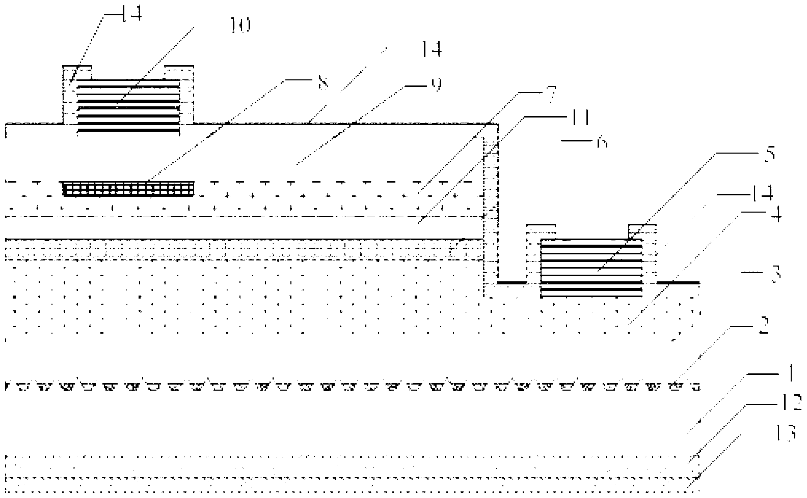
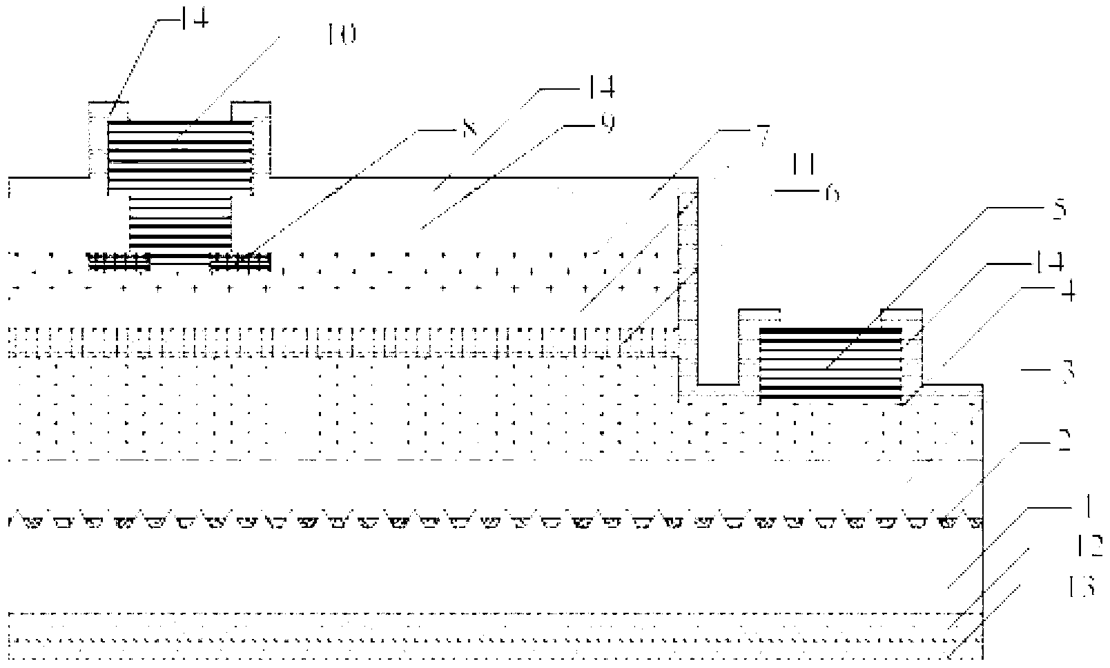
[0028] like figure 2 As shown, Embodiment 1 is a light-emitting diode with a current blocking layer. The common basic structure is: from bottom to top, it includes a substrate 1, a buffer layer 2, a non-doped GaN layer 3, an n-type GaN layer 4, and an n-type GaN layer. The n-electrode 5 formed on the GaN layer 4, the active layer 6, the p-type GaN layer 7, the current blocking layer 8, the transparent conductive layer 9 and the p-electrode 10 formed on the transparent conductive layer 9, in the transparent conductive layer 9 and The current blocking layer 8 is provided with an opening structure for enabling the p-electrode 10 to contact the p-type GaN layer 7 through the transparent conductive layer 9 and the openi...


PUM


Abstract

The invention relates to a light emitting diode with a current barrier layer. The light emitting diode comprises a substrate, a buffer layer, a non-doped GaN layer, an n-type GaN layer, an n electrode formed on the n-type GaN layer, an active layer, a p type GaN layer, a current barrier layer, a transparent conductive layer and a p electrode formed on the transparent conductive layer in turn from bottom to top. The light emitting diode is characterized in that pored structures are arranged on the transparent conductive layer and the current barrier layer, and the p electrode is in contact with the p type GaN layer through the pored structures on the transparent conductive layer and the current barrier layer. The light emitting diode prevents a current blocking effect caused by current flow right above the p electrode and increases the light intensity; the light emitted from the active layer is prevented from being absorbed right under the p electrode and the light extracting efficiency is increased; the adhesion of the electrode is increased and the risk of electrode falling is avoided; and the n electrode and the p electrode are in same color and convenience is brought to the automatic operation of a downstream chip packaging factory.

Description

technical field [0001] The invention relates to the technical field of photoelectric devices, in particular to a light emitting diode with a current blocking layer. Background technique [0002] The metal electrodes on the surface of the LED chip structure can make the current spread better, but the photons will be absorbed or reflected by the contacted metal when they are on the path of light emission, and the reflected photons may be absorbed, which is not conducive to improving the light output efficiency. . In order to solve this problem, the common practice in this industry is to add a current blocking layer in the LED chip structure to prevent the injected current from flowing directly under the P-pad electrode and expand its contact range outside the component. like figure 1 As shown, the traditional LED chip structure is sequentially provided with a substrate, a buffer layer, a non-doped GaN layer, an n-type GaN layer, an n-electrode formed on the n-type GaN layer,...

Claims


Application Information

Patent Timeline
Patent Type & Authority Applications(China)
IPC IPC(8): H01L33/14H01L33/38
Inventor 王汉华项艺杨新民靳彩霞董志江
Owner AQUALITE CO LTD
Why Eureka
Try Eureka