Through-silicon via (TSV) testing structure and TSV testing method

A technology of testing structure and testing method, applied in electromagnetic measuring device, electrical/magnetic diameter measurement, electrical components, etc., can solve the problem of ineffective testing, and achieve the effect of accurate, sensitive, convenient and quick measurement

Active Publication Date: 2015-04-29
SEMICON MFG INT (SHANGHAI) CORP
View PDF3 Cites 0 Cited by
  • Summary
  • Abstract
  • Description
  • Claims
  • Application Information

AI Technical Summary

Problems solved by technology

[0005] However, since the TSV runs through the entire wafer, the TSV will affect the nearby wafer structure and semiconductor devices, but there is no effective test for the impact of the TSV on the nearby wafer structure and semiconductor devices. semiconductor test structure

Method used


Image

  • Through-silicon via (TSV) testing structure and TSV testing method
  • Through-silicon via (TSV) testing structure and TSV testing method
  • Through-silicon via (TSV) testing structure and TSV testing method

Examples


Embodiment Construction

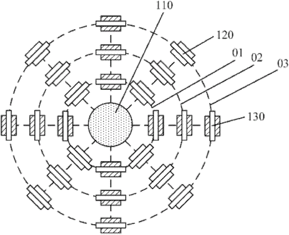
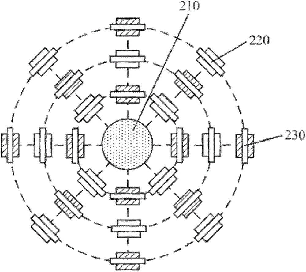
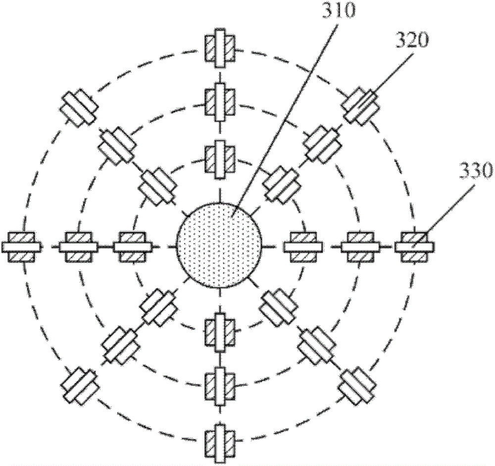
[0043] In the prior art, in order to realize three-dimensional stacking of chips, through-silicon vias penetrate the entire silicon substrate to realize the electrical connection between the upper and lower chips. Wherein, the TSV is filled with copper, and an isolation layer is formed between the copper and the silicon substrate to prevent copper from diffusing into the silicon substrate. However, when the temperature of the silicon substrate changes, due to the thermal expansion coefficient mismatch between the copper and the silicon substrate, it is easy to cause the TSV to generate tensile or compressive stress on the surrounding silicon substrate. The magnitude of the compressive stress is inversely proportional to the distance from the TSV, and the tensile or compressive stress changes the lattice constant of the channel region of the MOS transistor finally formed around the TSV, so that the current carrying The mobility of the electrons has changed, which affects the el...


PUM


Abstract

The invention provides a through-silicon via (TSV) testing structure and a TSV testing method. The TSV testing structure comprises a silicon substrate, a TSV penetrating through the silicon substrate, and a plurality of metal oxide semiconductor (MOS) transistors which are arranged around the TSV, wherein the MOS transistors surround the circle center of the TSV to form a plurality of concentric circular rings. Due to the fact that the MOS transistors of the TSV testing structure form the plurality of concentric circular rings in an enclosed mode, the electrical parameters of the MOS transistors in the different circular rings are compared with the electrical parameters of MOS transistors around which no TSVs are formed so that the radius of an isolation region which cannot be affected by the stress of the TSV is obtained, and the measurement is accurate, sensitive, convenient and rapid.

Description

technical field [0001] The invention relates to the technical field of semiconductor testing, in particular to a through-silicon via test structure and a test method for testing the radius of a through-silicon via isolation region. Background technique [0002] With the rapid development of portable electronic devices such as mobile phones, the size of portable electronic devices has become smaller and smaller, and the functions provided have become more and more extensive. Therefore, it is very necessary to improve the built-in chip without increasing the size of the device. level of integration. Since the feature size of semiconductor devices has become very small at present, it is becoming more and more difficult to increase the number of semiconductor devices in a two-dimensional structure. Therefore, three-dimensional packaging has become a method that can effectively improve chip integration. Current three-dimensional packaging includes die stacking based on gold wire...

Claims


Application Information

Patent Timeline
Patent Type & Authority Patents(China)
IPC IPC(8): H01L23/544H01L23/48G01B7/12
Inventor 冯军宏甘正浩
Owner SEMICON MFG INT (SHANGHAI) CORP
Why Eureka
Try Eureka