Manufacturing process of light emitting diode (LED) module group and LED module group

A technology of LED module and manufacturing process, which is applied in the direction of electrical components, circuits, semiconductor devices, etc., can solve the problems of high production cost and low light output rate, and achieve the effect of high production cost, low cost and simple production

Inactive Publication Date: 2013-05-08
HANGZHOU HPWINNER OPTO CORP
View PDF4 Cites 7 Cited by
  • Summary
  • Abstract
  • Description
  • Claims
  • Application Information

AI Technical Summary

Problems solved by technology

[0012] The purpose of the present invention is to provide a manufacturing process of LED modules to solve the technical problems of low light extraction rate and high production cost in t...

Method used


Image

  • Manufacturing process of light emitting diode (LED) module group and LED module group
  • Manufacturing process of light emitting diode (LED) module group and LED module group
  • Manufacturing process of light emitting diode (LED) module group and LED module group

Examples


Embodiment Construction

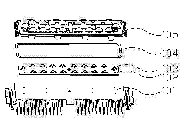
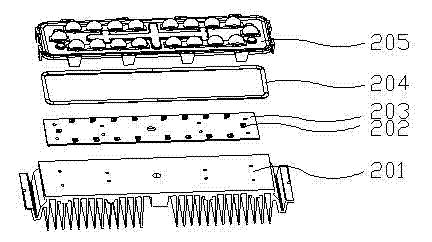
[0046] Such as figure 2 As shown, an LED module includes: a heat sink 201 , a circuit board 202 , an LED device 203 , a sealing silicone 204 , and a lens module 205 .

[0047] The LED device 203 includes an LED chip and a bracket, which are welded on the circuit board 202 . The LED device 203 does not include a light exit lens. The LED device 203 is directly welded on the circuit board 202, and the bottom of the circuit board 202 is in contact with the heat sink 201

[0048] The lens module 205 is covered on the LED device 203 , filled with molding colloid, and forms a sealed structure with the circuit board 202 and the heat sink 201 through the sealing silicone 204 . That is, the space between each pit of the lens module 205 and the LED device 203 is provided with molding colloid that matches the optical refractive index of the lens module 205, the LED device 203 is completely covered by the molding colloid and no air is left between them, and the lens mold A sealing ...


PUM


Abstract

A manufacturing process of a light emitting diode (LED) module group includes the following steps: (1), LED components without light-out lenses are welded on a circuit board; (2), the circuit board of the step one is fixed on a radiator, and the bottom of the circuit board is tightly attached to the radiator to form surface contact; (3), molding gel is filled in each concaved pit in the inner surface of an inverted lens module group and matched with the light refraction index of the lens module group; (4), the radiator of the step two is buckled on the lens module group in an inverted mode, the concaved pits filled with the gel correspond to the LED components and then is pressed tightly, and the LED components are completely coated with the molding gel and air is not residual between the LED components and the molding gel; (5), and the lens module group and the radiator are fixed to form the LED module group. Only the molding gel exists between the lens muddle group and an LED light source, the air is not included, light rays pass through a few media, transmittance is high, the filled gel is matched with the refraction index of the lens module group, reflection losses are few, and the light-out rate of the LED module group is improved. In addition, the LED light source only comprises a chip and an encapsulation support, the light-out lens is not included, and the cost is reduced.

Description

technical field [0001] The present invention relates to the field of semiconductor application and packaging, and more specifically relates to an LED (light emitting diode) module and its manufacturing process. Background technique [0002] With the development of LED chip technology and packaging technology, more and more LED products are used in the field of lighting, especially high-power white LEDs. Due to the characteristics of high light efficiency, long life, energy saving and environmental protection, suitable dimming control, and no mercury and other pollutants, LEDs have become a new generation of lighting sources after traditional light sources such as incandescent lamps and fluorescent lamps. [0003] Luminous efficiency is one of the most important indicators to measure the performance of LEDs, which characterizes the light output efficiency of LEDs and directly affects the energy-saving effect of LEDs. In order to increase the light output rate, the usual LED ...

Claims


Application Information

Patent Timeline
IPC IPC(8): H01L33/00H01L33/48H01L33/58H01L33/64
Inventor 吕华丽蔡建奇
Owner HANGZHOU HPWINNER OPTO CORP
Why Eureka
Try Eureka