

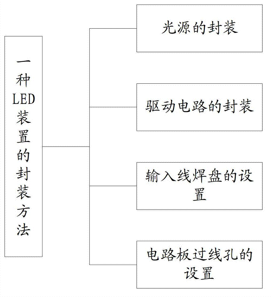
Packaging method of light-emitting diode (LED) device
A technology of LED device and packaging method, which is applied to electrical components, circuits, semiconductor devices, etc., can solve the problems of low luminous efficiency, waste of raw materials, and complicated packaging process, and achieves the advantages of simple packaging process, simplified installation process, and improved luminous efficiency. Effect
- Summary
- Abstract
- Description
- Claims
- Application Information
AI Technical Summary
Problems solved by technology
Method used
Image

Examples
Embodiment
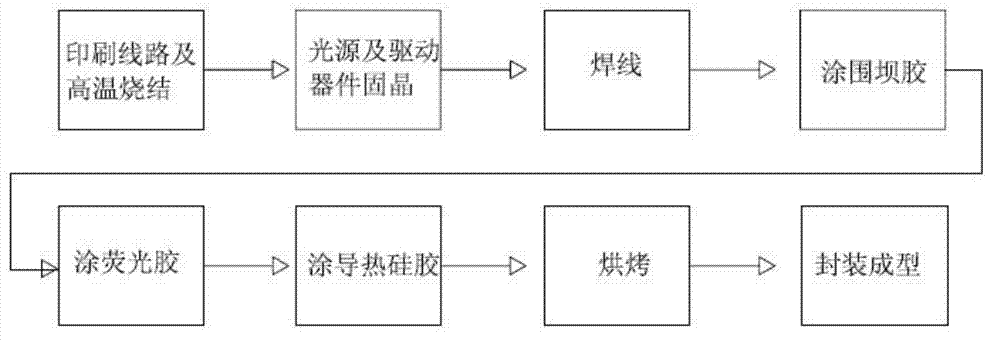
[0028] The specific implementation manner of the present invention will be described below in conjunction with the accompanying drawings.
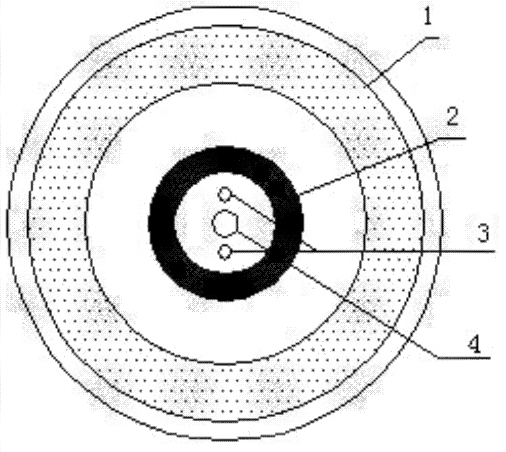
[0029] like figure 1 and figure 2 As shown, a packaging method for an LED device, comprising:
[0030] Packaging of the light source: the LED light source chip is directly packaged in the light source packaging area 1 of the ceramic substrate by COB packaging;
[0031] Packaging of the driving circuit: directly package all components of the driving circuit in the driving circuit packaging area 2 of the ceramic substrate with bare chips;
[0032] The setting of the input line pad 3: the input line pad 3 adopts the printed circuit technology, and is directly printed on the position of the input line pad 3 of the ceramic substrate;
[0033] The setting of circuit board wire hole 4: open a hole in the middle of the ceramic substrate, pass the input power line through this hole, and connect it to the input line pad 3.
[0034] Preferably, ...
PUM
 Abstract
Description
Claims
Application Information