Method and equipment for filling primer in semiconductor packaging

A technology of filling equipment and filling method, which is applied in the fields of semiconductor devices, semiconductor/solid-state device manufacturing, semiconductor/solid-state device components, etc., can solve the problem of low overall process efficiency, and achieve the effect of shortening the required time and reducing time-consuming

Active Publication Date: 2016-04-13
PEKING UNIV SHENZHEN GRADUATE SCHOOL
View PDF9 Cites 1 Cited by
  • Summary
  • Abstract
  • Description
  • Claims
  • Application Information

AI Technical Summary

Problems solved by technology

Another disadvantage is that while the primer flow time is reduced, it takes time to vent the cavity and evacuate or pressurize the device substrate
The most important thing is that underfill filling is still completed one device after another, and the overall process efficiency is not high

Method used


Image

  • Method and equipment for filling primer in semiconductor packaging
  • Method and equipment for filling primer in semiconductor packaging
  • Method and equipment for filling primer in semiconductor packaging

Examples


Embodiment Construction

[0033] The present invention will be further described in detail below through specific embodiments in conjunction with the accompanying drawings.

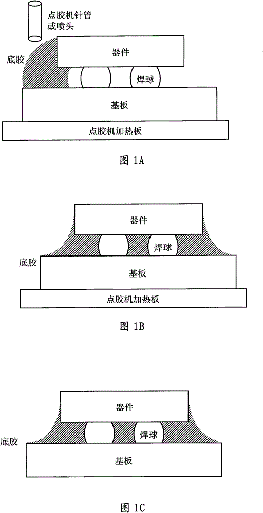
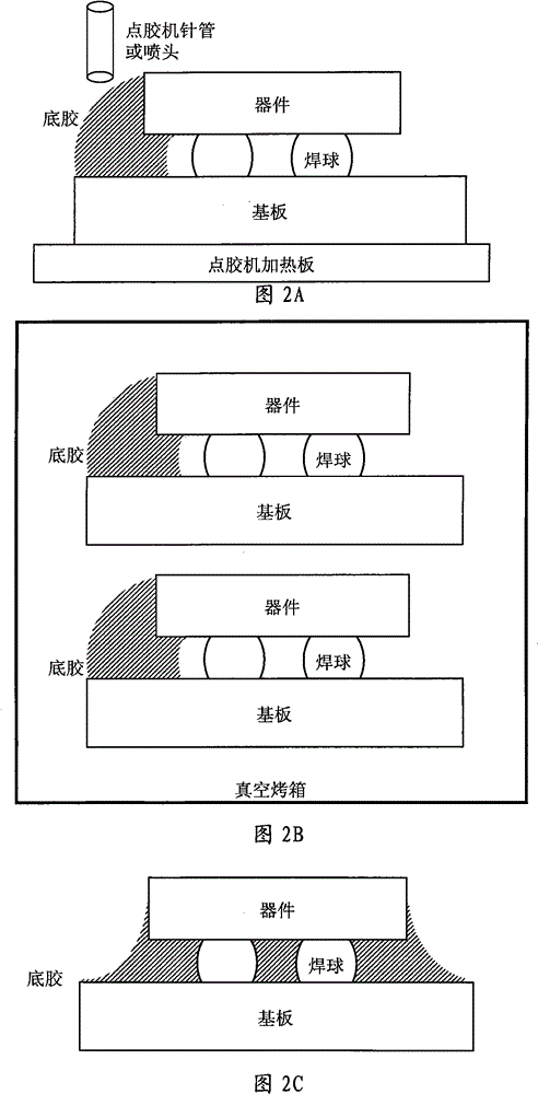
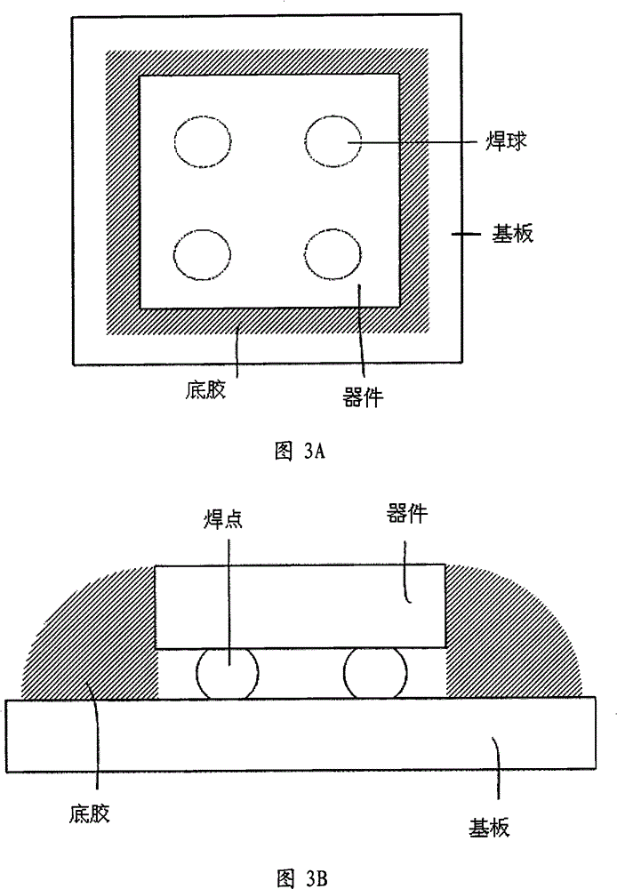
[0034] The invention relates to a method and equipment for filling primers in semiconductor packaging and other devices. Packaging herein refers to the interconnection of one or more semiconductor package devices with a printed circuit board substrate or interconnection between devices using solder and other bonding materials. see figure 1 , the traditional primer filling is to apply the primer on the edge of the packaged components on a machine, and then the primer flows through capillary action in the air environment and fills the gap between the substrate and the device, and finally the primer is in the Cured in a conventional air-heated oven. The main disadvantages of the traditional method are the long time or low production efficiency of the primer flow process for a single component, and the easy occurrence of voids due t...


PUM


Abstract

Glue (4) filling method and device in the semiconductor package is provided. The glue (4) is coated to one edge or four edges of semiconductor or chips on the substrate, the glue (4) is flowing between the chip and the substrate until the space is full filled. Several edges of device are coated glue (4) and the device is moved to the vacuum box, the glue (4) is batch flowing in the several devices so that the time of filling glue (4) is decreased and the production efficiency is increased. The glue (4) is solidified in the vacuum box and the air bubbles cancel during formed glue (4) time and the cavities cancel due to the gas volatilize during glue (4) solidified. The quality and the reliability of device glue (4) filling is increased.

Description

technical field [0001] The invention relates to a primer filling method and equipment in semiconductor packaging. Background technique [0002] Surface mount is currently one of the most popular packaging methods for assembling electronic devices on a substrate or printed circuit board (PCB). In this package, the surface mount device is interconnected with the substrate using multiple metal solder joints (such as lead-tin alloy), and there is a gap between the mount device and the substrate. If the thermal expansion coefficient (CTE) of the mounted device is different from that of the substrate, stress and strain will be generated in the solder joint when the temperature changes, and the stress and strain generated by the temperature change of the device during use will cause the solder joint to fatigue and fracture and fail. To solve this reliability problem, the common practice in the electronics industry is to fill the gap between the device and the substrate with primer...

Claims


Application Information

Patent Timeline
Patent Type & Authority Patents(China)
IPC IPC(8): H01L21/58
CPCH01L21/563H01L23/3157H01L24/16H01L24/83H01L2224/16225H01L2224/16227H01L2224/32225H01L2224/73204H01L2224/8109H01L2224/81855H01L2224/83104H01L2224/83194H01L2224/83986H01L2224/92125H01L2924/00014H01L2924/00H01L2924/00012H01L2224/0401
Inventor 金鹏卢基存
Owner PEKING UNIV SHENZHEN GRADUATE SCHOOL
Why Eureka
Try Eureka