Method, device and system of testing of chip frequency
A test method and chip technology, applied in the electrical field, can solve problems such as increased chip production costs, high cost, and complicated test methods, and achieve the effects of reducing production costs, improving reliability, and reducing the probability of mistesting
- Summary
- Abstract
- Description
- Claims
- Application Information
AI Technical Summary
Problems solved by technology
Method used
Image
Examples
Embodiment 1
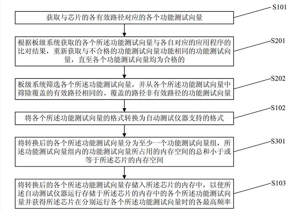
[0018] Embodiments of the present invention provide a method for testing chip frequency, such as figure 1 As shown, the method includes:
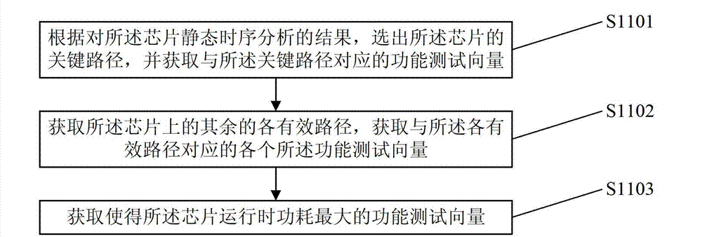
[0019] Step S101, acquiring each functional test vector corresponding to each test path of the chip, where the test path includes a critical path and an effective path;
[0020] A basic definition of a test vector is that a test vector is logic 1 and logic 0 data applied to a device pin every clock cycle for testing or manipulation. Logic 1s and 0s are represented by waveforms with timing characteristics and level characteristics, related to waveform shape, pulse width, pulse edge or slope, and position of rising and falling edges. In automated test language, these waveforms are represented by this formatted description of the rising edge, falling edge, and setup and hold time requirements of the device pins.
[0021] According to the different test vectors, it can be divided into functional test vectors and structural test vectors.
[0...
Embodiment 2
[0032] Embodiments of the present invention provide a method for testing chip frequency, such as figure 1 As shown, the method includes:
[0033] Step S101, acquiring each functional test vector corresponding to each test path of the chip, where the test path includes a critical path and an effective path;
[0034] A basic definition of a test vector is that a test vector is logic 1 and logic 0 data applied to a device pin every clock cycle for testing or manipulation. Logic 1s and 0s are represented by waveforms with timing characteristics and level characteristics, related to waveform shape, pulse width, pulse edge or slope, and position of rising and falling edges. In automated test language, these waveforms are represented by this formatted description of the rising edge, falling edge, and setup and hold time requirements of the device pins.
[0035] According to the different test vectors, it can be divided into functional test vectors and structural test vectors.
[0...
Embodiment 3
[0068] The embodiment of the present invention provides a chip frequency test device, such as Figure 4 As shown, the device includes:
[0069] an acquisition unit, which acquires each functional test vector corresponding to each test path of the chip, where the test path includes a critical path and an effective path;
[0070] A basic definition of a test vector is that a test vector is logic 1 and logic 0 data applied to a device pin every clock cycle for testing or manipulation. Logic 1s and 0s are represented by waveforms with timing characteristics and level characteristics, related to waveform shape, pulse width, pulse edge or slope, and position of rising and falling edges. In automated test language, these waveforms are represented by this formatted description of the rising edge, falling edge, and setup and hold time requirements of the device pins.
[0071] According to the different test vectors, it can be divided into functional test vectors and structural test v...
PUM
 Abstract
Description
Claims
Application Information
 - R&D
- Intellectual Property
- Life Sciences
- Materials
- Tech Scout
- Unparalleled Data Quality
- Higher Quality Content
- 60% Fewer Hallucinations
Browse by: Latest US Patents, China's latest patents, Technical Efficacy Thesaurus, Application Domain, Technology Topic, Popular Technical Reports.
© 2025 PatSnap. All rights reserved.Legal|Privacy policy|Modern Slavery Act Transparency Statement|Sitemap|About US| Contact US: help@patsnap.com


