
Printed circuit bard (PCB) for preventing electrostatic discharge

A kind of PCB circuit board, electrostatic discharge technology, applied in the direction of static electricity, printed circuit parts, electrical measuring instrument parts, etc., can solve the problems of large size of scanning card, sharp increase in cost, unacceptable, etc., to improve test accuracy , safe to use, cost-saving effect

Inactive Publication Date: 2013-06-05
SHENZHEN MASONE ELECTRONICS
View PDF2 Cites 6 Cited by
  • Summary
  • Abstract
  • Description
  • Claims
  • Application Information

AI Technical Summary

Problems solved by technology

And each test point must withstand the rated test voltage of 300V when it works normally, so if a dedicated TVS device is added to each test point, the size of the entire scanning card will increase and the cost will increase dramatically
therefore unrealistic and unacceptable

Method used


Image

  • Printed circuit bard (PCB) for preventing electrostatic discharge
  • Printed circuit bard (PCB) for preventing electrostatic discharge
  • Printed circuit bard (PCB) for preventing electrostatic discharge

Examples


Embodiment Construction

[0023] Below in conjunction with accompanying drawing and specific embodiment the present invention will be further described:

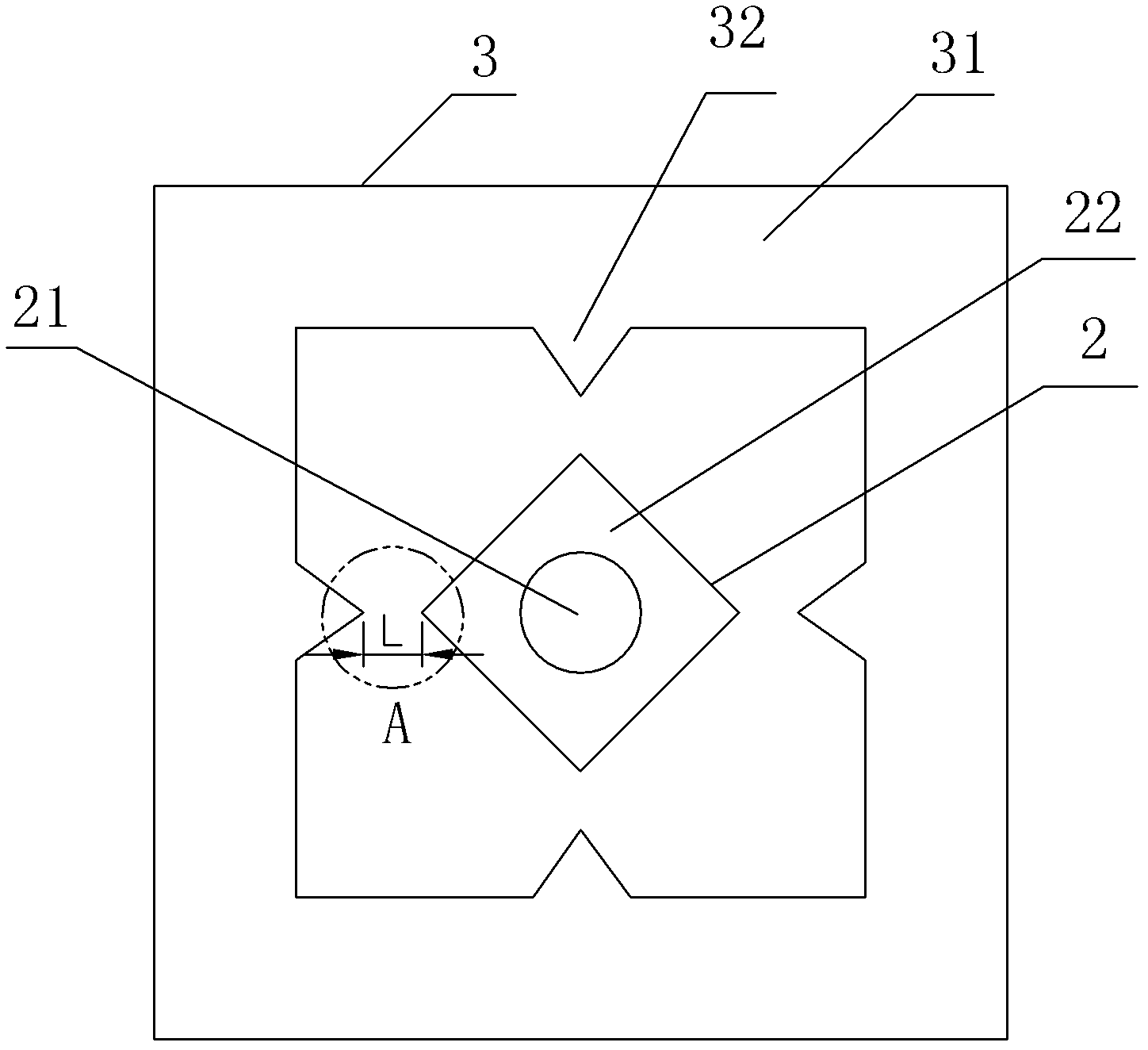
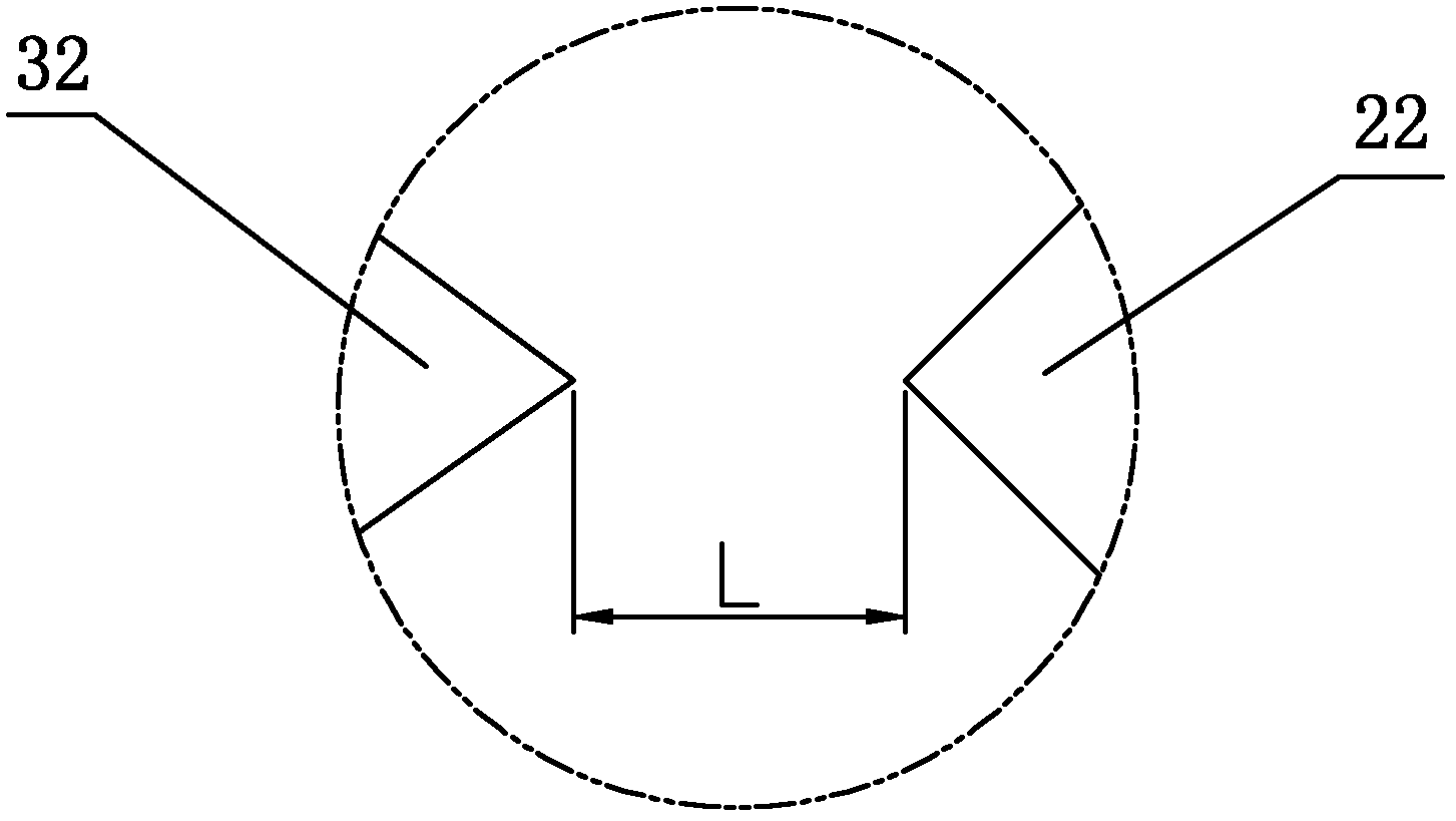
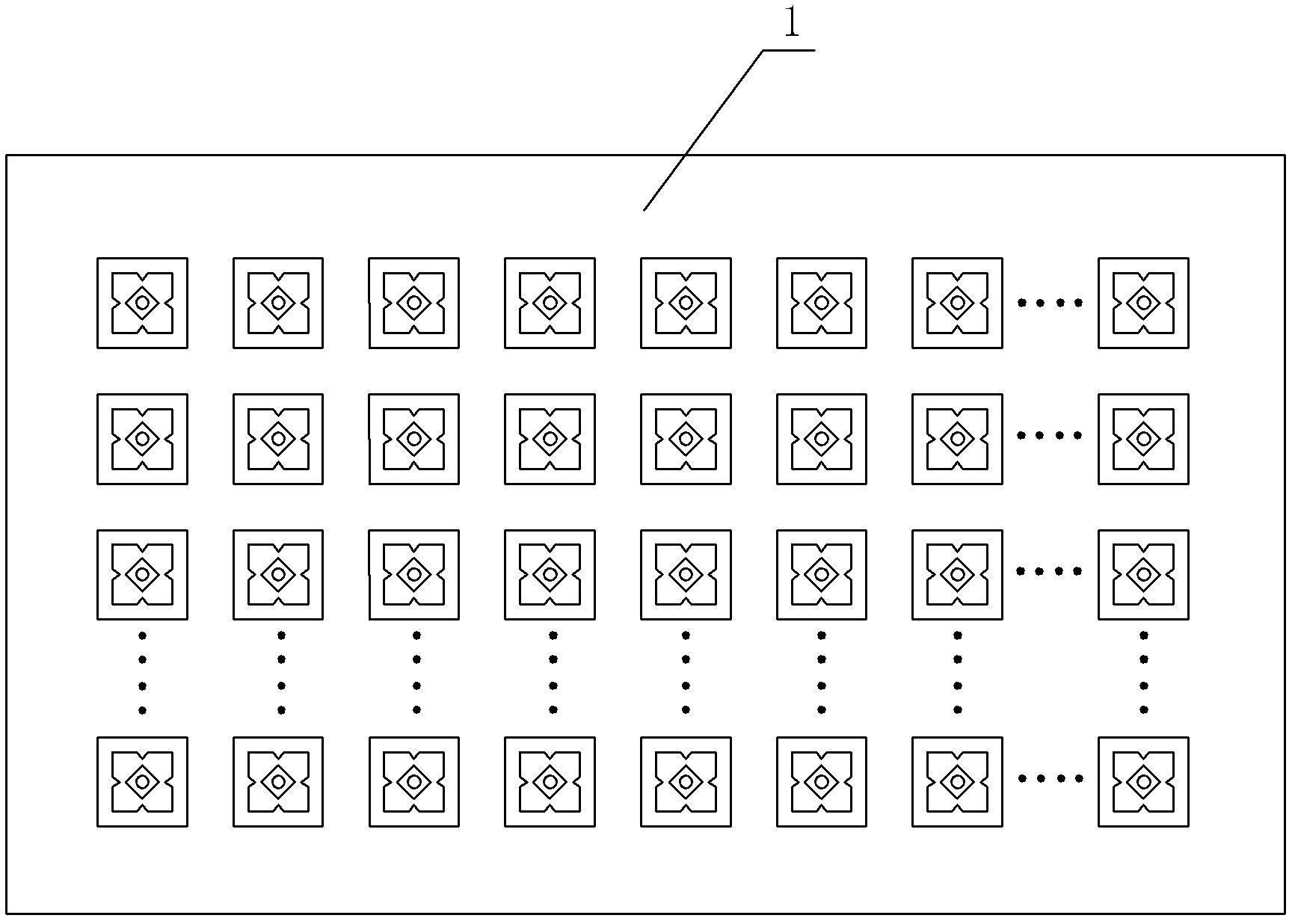
[0024] refer to Figure 1 to Figure 4 As shown, the present invention discloses a PCB circuit board for preventing electrostatic discharge, which includes a substrate 1; the substrate 1 is made of an insulating material; a circuit pattern formed on the substrate 1; There is at least one discharge pin 2 for connecting with external electrical signals, and the number of discharge pins 2 is set according to the number of specific test points. Each discharge pin 2 is distributed on the substrate in an array, and each discharge pin 2 At least one sharp corner is provided. In this embodiment, four sharp corners are arranged on each discharge pin 2, and a copper skin 3 is laid on the periphery of the discharge pin 2 on the substrate 1. The copper skin 3 has a The sharp corners of the discharge pin 2 have the same number of sharp corners, and the sharp corn...


PUM


Abstract

The invention discloses a printed circuit board (PCB) for preventing electrostatic discharge. The PCB comprises a substrate and circuit patterns, wherein the substrate is made of insulating materials. The PCB is characterized in that at least one discharging pin for connecting external electric signals is arranged on the substrate, at least one tip is arranged on the discharging pin, copper skin is overlaid on the periphery of the discharging pin on the substrate and provided with sharp tips with the same quantity of sharp tips on the discharging pin, the sharp tips on the copper skin correspond to the sharp tips on the discharging pin, discharging spaces are arranged between tip ends of the corresponding sharp tips on the copper skin and the discharging pins, and the copper skin is electrically connected with the ground. The PCB has the advantages that during testing, damage and punch-through on electrical elements in a scanning card caused by an external electro spark detector (ESD) can be avoided, well protection on the inner circuit can be achieved, and interference on channel signals (namely a testing point channel) caused by the ESD of the PCB can be reduced.

Description

【Technical field】 [0001] The invention relates to a PCB circuit board, in particular to a PCB circuit board for preventing electrostatic discharge inside a scanning card used in PCB board detection. 【Background technique】 [0002] In PCB optical circuit board testing machines, ICT testing machines, ATE testing equipment and semiconductor testing equipment and other related fields, the core test / measurement components will use various forms of scanning cards (or called switch cards), scanning cards according to The CPU commands to switch various electrical signals (including various power sources, signal sources, instruments, etc.), so that these signals are applied to the DUT (device under test) to complete the measurement of various electrical signals. The following is an example of a typical PCB optical line tester: [0003] The PCB optical circuit board testing machine applies the voltage and current set by the program between any two points of the PCB optical board to b...

Claims


Application Information

Patent Timeline
Patent Type & Authority Applications(China)
IPC IPC(8): H05K1/02H05F3/02G01R1/067
Inventor 李新学刑明林王芳夏春石磊杨朝辉
Owner SHENZHEN MASONE ELECTRONICS
Learn More