

Substrate processing device
A substrate processing device and processing liquid technology, applied in decorative art, technology for producing decorative surface effects, electrical components, etc., can solve the problem of rising concentration of processing liquid, inability to measure concentration, unstable etching speed of silicon nitride film, etc. problem, to achieve the effect of reducing the amount of etching, increasing the amount of etching, and stabilizing the etching
- Summary
- Abstract
- Description
- Claims
- Application Information
AI Technical Summary
Problems solved by technology
Method used
Image

Examples
Embodiment Construction
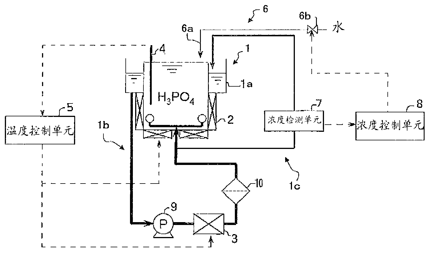
[0026] The substrate processing apparatus of the present invention heats a processing liquid obtained by mixing a chemical liquid and a diluent, and processes a substrate by immersing it in the processing liquid. In this embodiment, the following device is used as an example for description, that is, the treatment liquid is a phosphoric acid solution containing phosphoric acid as a chemical liquid and water as a diluent, the phosphoric acid solution is heated, and a substrate (such as a Silicon wafers) are dipped into the phosphoric acid solution for etching.
[0027] This substrate processing apparatus includes a processing tank 1 for storing a phosphoric acid solution. A recovery tank 1 a for recovering phosphoric acid solution overflowing from the treatment tank 1 is provided around the treatment tank 1 . The phosphoric acid solution recovered from the recovery tank 1a is returned to the treatment tank 1 through the circulation pipe 1b.
[0028] A circulation pump 9 , a h...
PUM
 Abstract
Description
Claims
Application Information