Flash memorizer and manufacturing method thereof

A flash memory and charge storage technology, applied in the field of memory, can solve problems such as reducing the storage reliability of flash memory, and achieve the effects of ensuring storage reliability, improving stability, and maintaining fast data access.

Active Publication Date: 2013-06-19
INST OF MICROELECTRONICS CHINESE ACAD OF SCI
View PDF3 Cites 1 Cited by
  • Summary
  • Abstract
  • Description
  • Claims
  • Application Information

AI Technical Summary

Problems solved by technology

[0006] The present invention provides a flash memory, which solves the problem of lowering the storag...

Method used


Image

  • Flash memorizer and manufacturing method thereof
  • Flash memorizer and manufacturing method thereof
  • Flash memorizer and manufacturing method thereof

Examples


Embodiment Construction

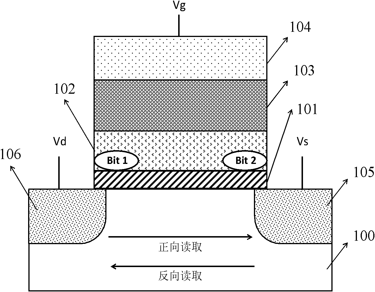
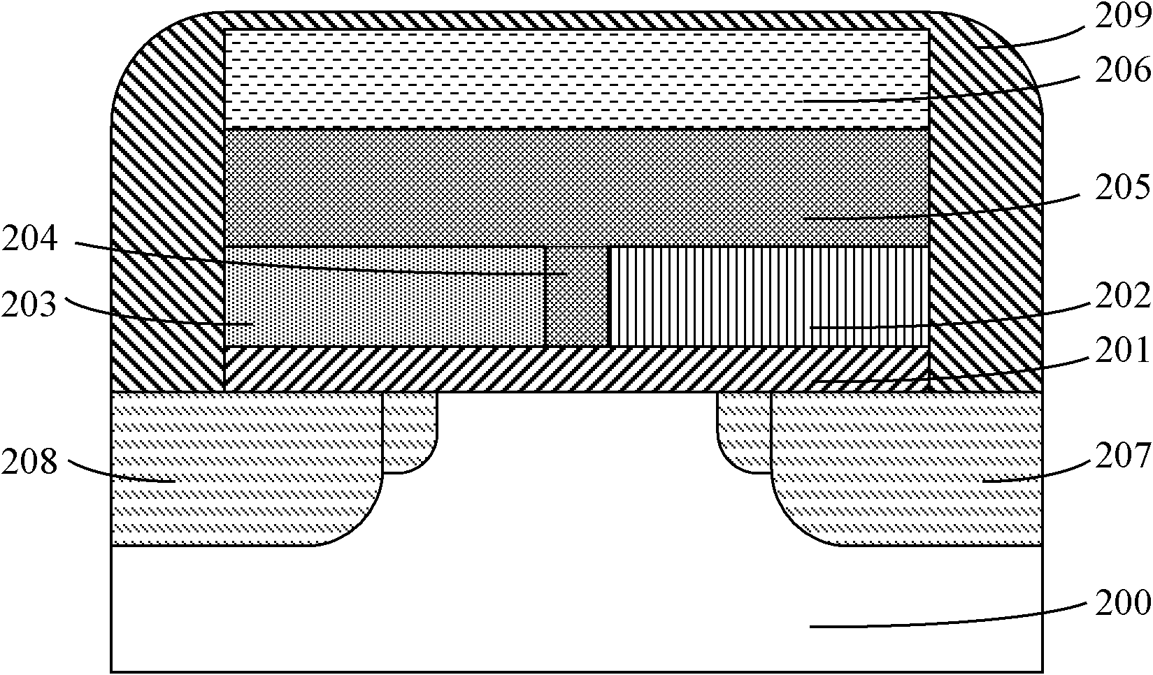
[0046]The NROM structure flash memory utilizes the localized storage characteristics of charges to store charges at multiple locations in the same charge storage layer, which increases the storage density of the memory. However, as the size of the memory continues to decrease, when programming the existing NROM-structure flash memory, it may cause crosstalk and source injection of information stored in multiple locations, reducing the storage reliability of the memory.

[0047] Based on the above reasons, the present invention proposes a flash memory. The charge storage layer is made into two mutually independent charge storage areas, and an isolation dielectric area is used to isolate the two charge storage areas. The material of the isolation dielectric area adopts a conductive lower rate materials. Compared with the existing NROM structure memory, due to the addition of the isolation dielectric region, a higher energy barrier is formed between the two storage regions, so th...


PUM


Abstract

The invention provides a flash memorizer. A charge storage layer of the memorizer is divided into two charge storage areas by an isolation medium area. The conductivity of the isolation medium area is smaller than the conductivity of the two charge storage areas. Materials of the two charge storage areas are different. Correspondingly, the invention further provides a flash memorizer manufacturing method. The isolation medium area with the smaller conductivity is adopted by the charge storage layer of the flash memorizer to isolate the two charge storage areas from each other. Stored charge interference between the two charge storage areas can be restrained, and the storage reliability of the memorizer is guaranteed. In addition, one charge storage area is made of metal nitride nanocrystalline materials, and the other charge storage area is made of non-nanocrystalline semiconductor materials with higher dielectric constant. Consequently, the influence of source injection phenomena on the storing reliability of the memorizer can be avoided in the programming process.

Description

technical field [0001] The invention relates to the technical field of memory, in particular to a flash memory capable of multi-value storage and a manufacturing method thereof. Background technique [0002] With the increase of wireless communication data traffic and the improvement of the integration of multimedia equipment, the requirements for embedded storage are increasing. While requiring high-speed data access, it is also required to increase storage density. All of these put forward new requirements for the flash storage technology of the NOR array architecture. The flash memory technology of the NOR array architecture is mainly used in embedded storage, and nanocrystalline memory occupies an important position in the NOR embedded storage technology due to its fast programming and erasing speed. At the same time, since the storage capacity required by the current communication is increasing day by day, this requires the storage density of the memory to be further i...

Claims


Application Information

Patent Timeline
IPC IPC(8): H01L27/115H01L21/8247
Inventor 刘明王晨杰霍宗亮张满红刘璟谢常青王永
Owner INST OF MICROELECTRONICS CHINESE ACAD OF SCI
Why Eureka
Try Eureka