Ray detector and manufacturing method thereof

A ray detector and substrate technology, applied in the field of detectors, can solve problems such as complex production process, long production cycle, and low sensitivity, and achieve the effects of improving sensitivity, reducing production cost, and improving production efficiency

Active Publication Date: 2013-06-19
BEIJING BOE OPTOELECTRONCIS TECH CO LTD
View PDF4 Cites 16 Cited by
  • Summary
  • Abstract
  • Description
  • Claims
  • Application Information

AI Technical Summary

Problems solved by technology

[0017] Embodiments of the present invention provide a radiation detector and a manufacturing method thereof, which are used to solve the problems of complex manufacturing process, long manufacturing cycle, low sensitivity, and high power consumption of the radiation detector in the prior art

Method used


Image

  • Ray detector and manufacturing method thereof
  • Ray detector and manufacturing method thereof
  • Ray detector and manufacturing method thereof

Examples


Embodiment Construction

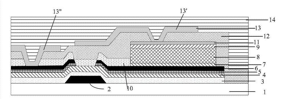
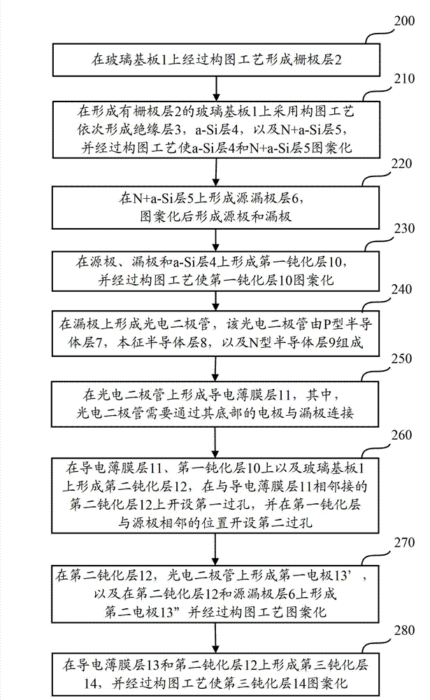
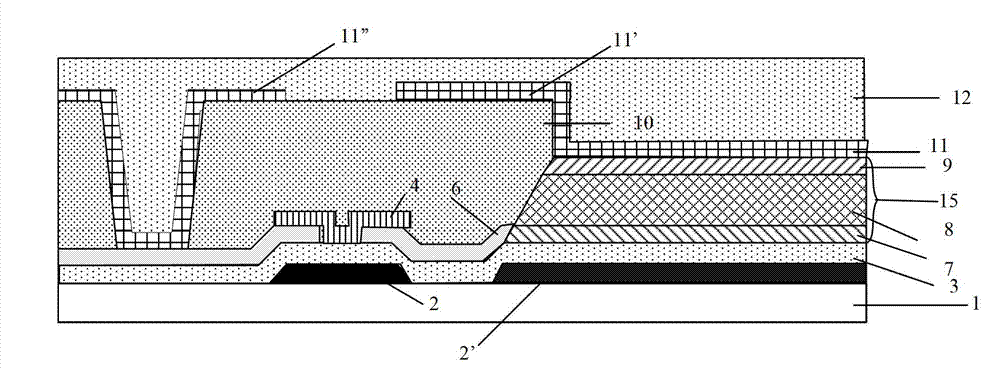
[0046] In order to solve the problems of complex manufacturing process, long manufacturing cycle, low sensitivity and high power consumption of the radiation detector existing in the prior art.

[0047] In the embodiment of the present invention, a gate layer and an insulating layer are sequentially formed on the substrate, and a photodiode and a source-drain layer are formed on the substrate on which the insulating layer is formed; connected; forming an active layer on the above-mentioned source-drain layer, so that the active layer is in contact with the insulating layer; forming a first passivation layer on the above-mentioned active layer and on the above-mentioned source-drain layer, and A via hole is opened on the first passivation layer; on the photodiode, a conductive film layer is formed on the first passivation layer and in the via hole, and a second passivation layer is formed on the conductive film layer. Compared with the prior art, the technical solution of the i...


PUM


Abstract

The invention discloses a ray detector and a manufacturing method thereof. A grid layer and an insulating layer are sequentially formed on a substrate, a photoelectric diode and a source drain layer are formed on the substrate with the insulating layer, a drain of the source drain layer is connected with the photoelectric diode, an active layer is formed on the source drain layer and contacts with the insulating layer, a first passivation layer is formed on the active layer and the source drain layer, a conductive film layer is formed on the photoelectric diode, the source drain layer and the first passivation layer, and a second passivation layer is manufactured on the conductive film layer. By the aid of the technical scheme, compared with the prior art, the ray detector has the advantages that masking frequency is decreased, production cycle is effectively shortened, production efficiency is improved, manufacturing cost is reduced, the sensitivity of the ray detector is improved, and power consumption of the ray detector is reduced.

Description

technical field [0001] The invention relates to the technical field of detectors, in particular to a radiation detector and a manufacturing method thereof. Background technique [0002] The functional device that completes the photoelectric conversion of image information is called a photoelectric image detector (or a photoelectric image sensor). The flat-panel radiation detector is a kind of photoelectric image detector, which is often used in the medical field. For example, flat-panel ray detectors detect X-rays passing through the human body, and display the intensity distribution of X-rays on the monitor in different gray scales, so that the results of X-ray detection of the human body can be seen more intuitively. [0003] see figure 1 As shown, it is a schematic structural diagram of a radiation detector in the prior art. The radiation detector includes a thin film transistor (Thin Film Transistor, TFT) and a photodiode, wherein, the TFT usually includes a gate, a so...

Claims


Application Information

Patent Timeline
Patent Type & Authority Applications(China)
IPC IPC(8): H01L27/146
CPCH01L27/14658
Inventor 田宗民阎长江谢振宇
Owner BEIJING BOE OPTOELECTRONCIS TECH CO LTD
Why Eureka
Try Eureka