
Advanced process control method of wet etching process

A wet etching and etching technology, applied in chemical instruments and methods, crystal growth, post-processing details, etc., can solve problems such as inability to reduce film thickness changes

Inactive Publication Date: 2013-06-26
SEMICON MFG INT (SHANGHAI) CORP
View PDF3 Cites 11 Cited by
  • Summary
  • Abstract
  • Description
  • Claims
  • Application Information

AI Technical Summary

Problems solved by technology

[0005] However, since the wet etching process flow is fixed, it cannot reduce the film thickness variation after the wet etching process

Method used


Image

  • Advanced process control method of wet etching process
  • Advanced process control method of wet etching process
  • Advanced process control method of wet etching process

Examples


Embodiment 1

[0049] to be removed using a conventional wet etch process film to get The target film thickness for such a process as an example.

[0050] The target film thickness obtained by conventional methods is The wafer is placed on the workbench.

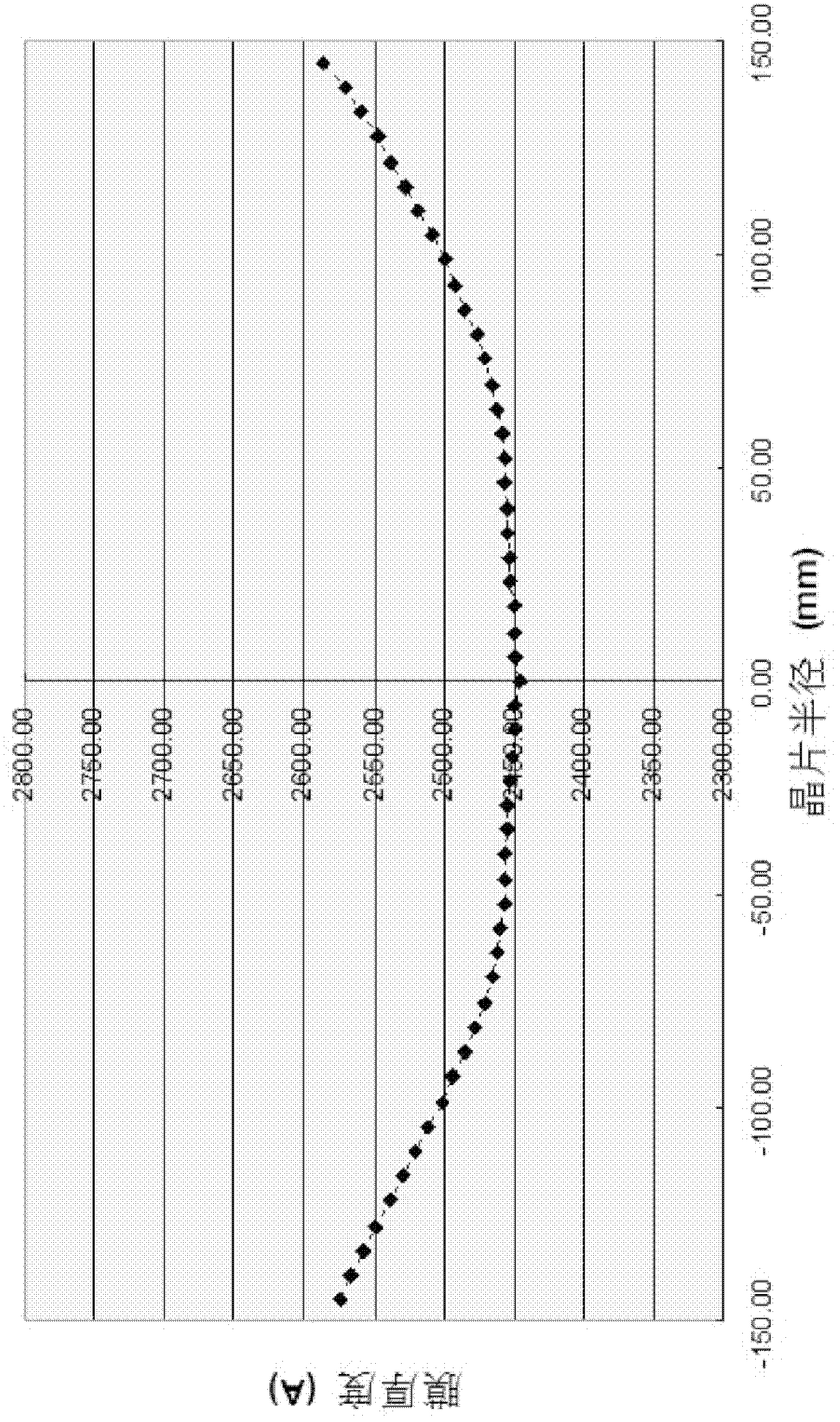
[0051] Utilize the Aleris model machine platform of KLA-Tencor Company to measure the linear film thickness of the film before wet etching, as figure 2 shown.

[0052] The resulting data is transmitted to a controller which can be interfaced with a computer for processing, displaying and / or storing the data. The computer compares the full image or linear film thickness of the input film with the target film thickness after wet etching, determines the actual target wet etching curve, and outputs the parameters of the etching process to the controller. When the value obtained by subtracting the target film thickness after wet etching from the full image or linear film thickness of the film before wet etching is less than 0, the output...

Embodiment 2

[0059] Utilize and the target film thickness of the same batch of embodiment 1 is wafers for experiments. The wet etching process was carried out in the same manner as in Example 1, except that the advanced process control method of Example 1 was not implemented, but the conventional etching process was directly performed (the etching time was fixed at 270s).

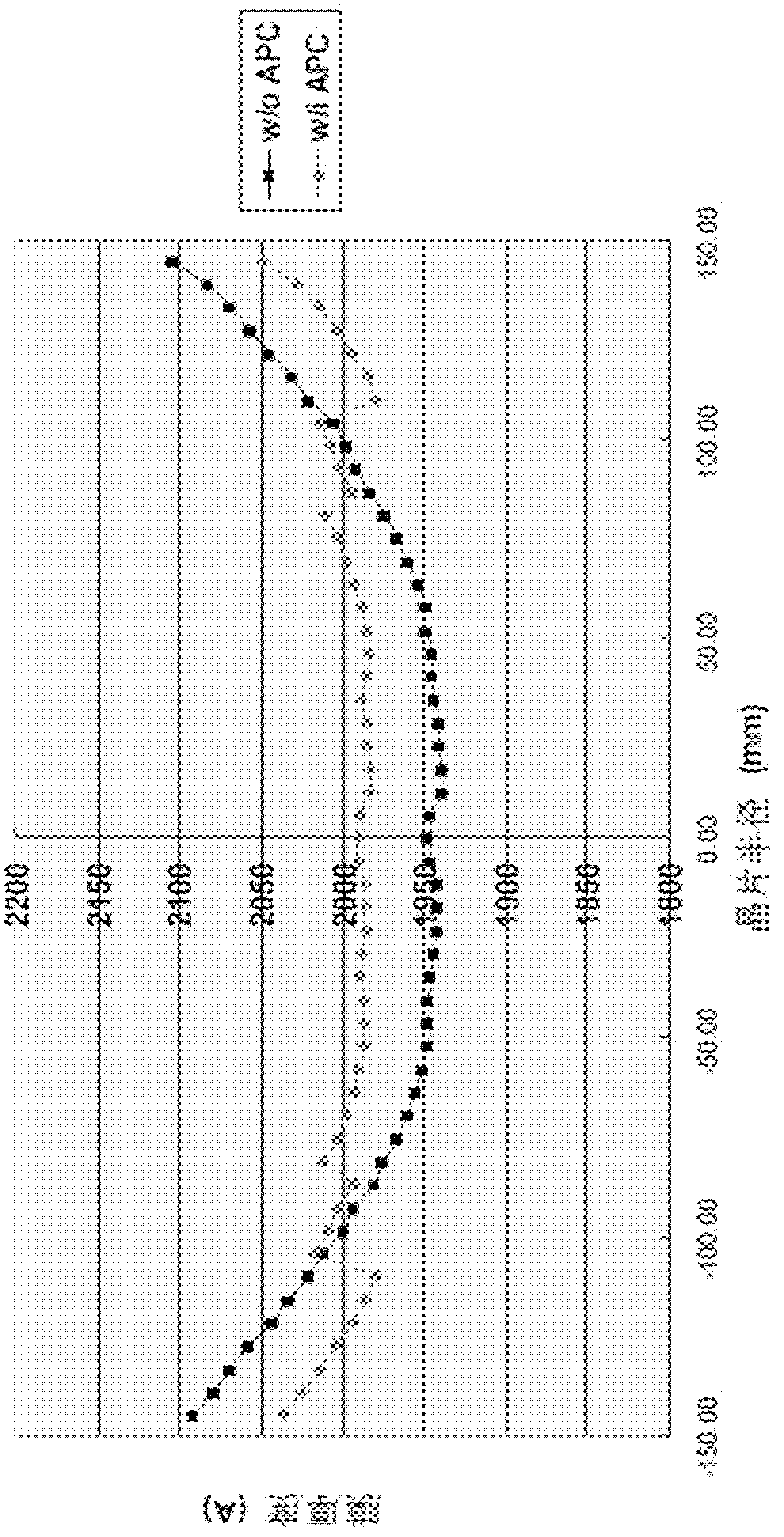
[0060] Utilize the Aleris model machine platform of KLA-Tencor Company to measure the linear film thickness of the film after wet etching, as image 3 Middle curve w / o APC is shown.

[0061] Table 1

[0062]

[0063] Table 1 shows the linear film thickness under different conditions, it can be seen that before etching, the actual value of the average film thickness is lower than the target value by about where the difference between the maximum value (wafer edge) and the minimum value (wafer center) is The standard deviation (STD) of the film thickness was 41.97, and the in-chip inhomogeneity % (U%) was 2.83, ...


PUM


Abstract

The invention relates to an advanced process control method of a wet etching process. The method comprises the following steps: carrying out measurement through a measuring device so as to obtain the total graph or linear film thickness of a wet etching front-film; subtracting the thickness of a target film subjected to wet etching, and determining an actual target wet etching curve; and determining an etching process to carry out etching according to the obtained actual target wet etching curve.

Description

technical field [0001] The invention relates to an advanced process control method of a wet etching process. Background technique [0002] In device processing in recent years, a wet etching process of a wafer by a spin etching device for the purpose of improving the mechanical strength of the chip or improving the electrical and thermal characteristics has been widely used. [0003] As CMOS shrinks to 32nm or smaller, how to control wafer variation becomes more and more important. But traditional film deposition steps, such as furnace and CVD, have thicker films at the edge of the wafer than at the center of the wafer. Amount of circle etch. [0004] Monolithic wet etch tools use a rotating wet clean method that enables control of the amount of wet etch at various radii from the center of the wafer. [0005] However, since the wet etching process flow is fixed, film thickness variation after the wet etching process cannot be reduced. If the film thickness is not uniform...

Claims


Application Information

Patent Timeline
IPC IPC(8): C23F1/00C23F1/08C30B33/10
Inventor 刘佳磊
Owner SEMICON MFG INT (SHANGHAI) CORP
Learn More