Grid driving circuit, display panel and display device

A gate drive circuit and display panel technology, applied in the fields of gate drive circuits, display panels and display devices, can solve the problems of gate drive signal distortion, different on-times, increased process complexity and cost, etc. Signal distortion, detrimental effects reduction, effects of detrimental effects mitigation

Active Publication Date: 2013-06-26
BOE TECH GRP CO LTD +1
View PDF4 Cites 10 Cited by
  • Summary
  • Abstract
  • Description
  • Claims
  • Application Information

AI Technical Summary

Problems solved by technology

And this RC delay will affect the signal transmission
[0006] like figure 1 As shown, it is assumed that the left side is close to the gate drive circuit, Von is the voltage corresponding to the TFT conduction, from figure 1 It can be found that at the end close to the gate drive circuit, the gate drive signal is basically not distorted, but at the end far away from the gate drive circuit, the distortion of the gate drive signal is very serious, and this distortion will lead to The conduction time of the TFT is different, which leads to inconsistent charging time of the pixel electrode, which has an adverse effect on the display
[0007] In the prior art, the adverse effects of RC delay are generally reduced by improving the material, shape, and size of the grid lines, such as using low-resistivity materials, increasing the width and thickness of the grid lines to reduce resistance, reduce The overlapping area of ​​gate lines and other conductive layers, etc., but these methods will undoubtedly affect the manufacturing process of the display panel, increasing the complexity and cost of the process

Method used


Image

  • Grid driving circuit, display panel and display device
  • Grid driving circuit, display panel and display device
  • Grid driving circuit, display panel and display device

Examples


Embodiment Construction

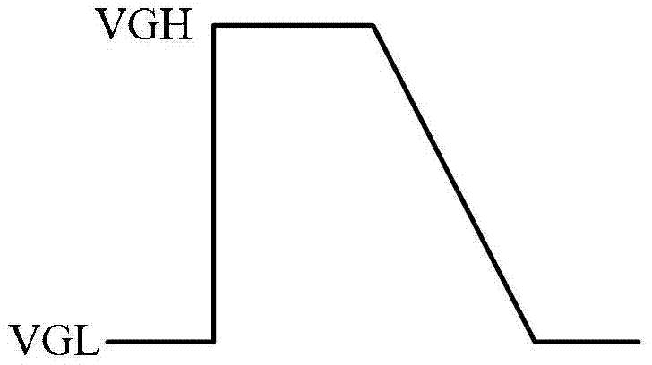
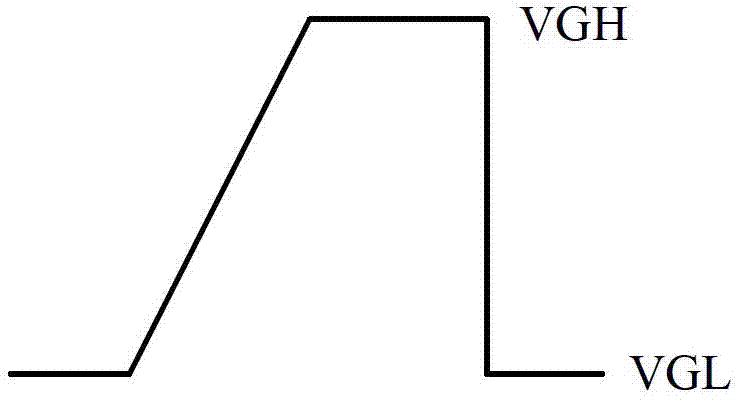
[0034] In the embodiment of the present invention, an improvement is made at one end of the gate drive circuit, so that the gate line drive signal generated by the gate drive circuit is no longer a square wave signal, but a signal with a chamfered waveform, which can reduce the The signal distortion caused by the delay can reduce the adverse effects of the RC delay.

[0035] Before describing the embodiments of the present invention in detail, some concepts involved in the embodiments of the present invention will be described in detail, so as to better understand the embodiments of the present invention.

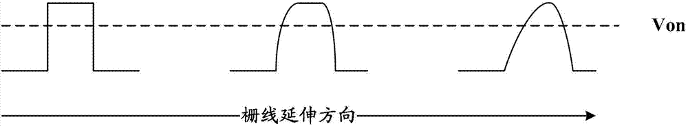
[0036] Generally, in a common gate driving device, the output to the gate line is as follows figure 1 The square wave signal shown on the left.

[0037] The so-called signal with a clipped waveform refers to:

[0038] On the rising edge of the driving signal, the voltage does not jump directly from VGL to VGH, but starts from VGL and rises to VGH after a certain period of...


PUM


Abstract

The embodiment of the invention discloses a grid driving circuit, a display panel and a display device. The grid driving circuit is used on the display panel and characterized by comprising a signal generating circuit and at least one signal, wherein the signal generating circuit is used for generating a grid line driving signal for driving a grid line positioned in the display panel, and the at least one signal enables the driving signal to have cutting angle waveform. The grid driving circuit, the display panel and the display device provide a scheme for weakening the negative influence caused by RC delay from the perspective of a signal source.

Description

technical field [0001] The invention relates to the driving of a display panel, in particular to a grid driving circuit, a display panel and a display device. Background technique [0002] The display device is a flat panel display widely used at present. Compared with other display methods, it has the advantages of low power consumption, light weight, and no radiation. [0003] A display device generally includes an array substrate, a color filter substrate, and a liquid crystal layer filled between the array substrate and the color filter substrate. The display area on the array substrate includes a plurality of sub-pixel areas, and each sub-pixel area is generally formed by crossing and surrounding two gate lines (scanning lines) and two data lines. [0004] A thin film transistor serving as a switching device and a pixel electrode are disposed inside the sub-pixel area. By controlling the voltage applied to the common electrode and / or the pixel electrode on the color f...

Claims


Application Information

Patent Timeline
Patent Type & Authority Applications(China)
IPC IPC(8): G09G3/36G09G3/20
CPCG09G3/3677
Inventor 许益祯孙志华吴行吉汪建明张亮
Owner BOE TECH GRP CO LTD
Why Eureka
Try Eureka