Semiconductor device and forming method thereof

A semiconductor and device technology, applied in the field of semiconductor devices and their formation, can solve the problems of large RC effect and poor performance of semiconductor integrated circuits, etc., and achieve the effect of small RC effect, small K value and good quality

Active Publication Date: 2014-11-05
SEMICON MFG INT (SHANGHAI) CORP
View PDF10 Cites 0 Cited by
  • Summary
  • Abstract
  • Description
  • Claims
  • Application Information

AI Technical Summary

Problems solved by technology

[0010] However, the RC effect of semiconductor devices using the prior art is still large, and the performance of semiconductor integrated circuits is poor

Method used


Image

  • Semiconductor device and forming method thereof
  • Semiconductor device and forming method thereof
  • Semiconductor device and forming method thereof

Examples


Embodiment Construction

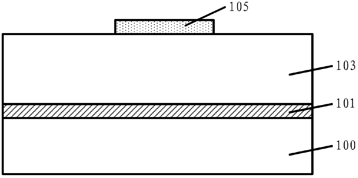
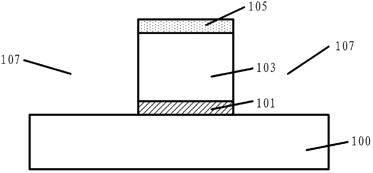
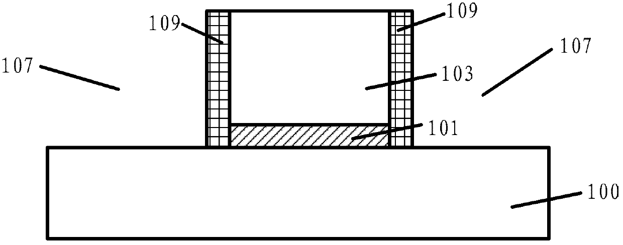
[0045] As mentioned in the background, the RC effect of the semiconductor device in the prior art is still relatively large, and the performance of the semiconductor integrated circuit is poor.

[0046] After research, the inventors found that in the prior art, when the opening is formed, if the size (width) of the opening is too large, the material used to form the insulating layer will fall into the opening when the insulating layer is subsequently formed, making it difficult to deposit the insulating layer. , it is difficult to form an insulating layer covering the metal line layer and across the opening, and even if the insulating layer is formed, the quality of the air gap is greatly affected. Therefore, limited by the subsequent deposition process, the size (width) of the air gap formed in the prior art is usually small. The small-sized air gap can reduce the K value in the interconnection structure is relatively limited, the RC effect of the semiconductor device is stil...


PUM

PropertyMeasurementUnit
widthaaaaaaaaaa
widthaaaaaaaaaa

Abstract

A forming method of a semiconductor device comprises the steps of providing a substrate, and enabling a first interlayer dielectric layer, a second interlayer dielectric layer and a groove penetrating through the thicknesses of the interlayer dielectric layers to be sequentially formed on the surface of the substrate; processing part of the first interlayer dielectric layer and the second interlayer dielectric layer on a side wall of the groove, respectively forming a first sacrificial layer and a second sacrificial layer, and enabling the width of the first sacrificial layer to be larger than that of the second sacrificial layer; after forming the first sacrificial layer and the second sacrificial layer, filling the groove to form a metal wire layer; after forming the metal wire layer, removing the first sacrificial layer and the second sacrificial layer to form an opening which comprises a first auxiliary opening at the bottom and a second auxiliary opening at the top, and enabling the opening diameter of the first auxiliary opening to be larger than that of the second auxiliary opening; and forming an insulating layer which is covered on the second interlayer dielectric layer and striding the opening. Correspondingly, the invention further provides the semiconductor device formed by adopting the method. Resistance capacitance (RC) effect is low, and performance of a semiconductor integrated circuit is good.

Description

technical field [0001] The invention relates to the technical field of semiconductor manufacturing, in particular to a semiconductor device and a forming method thereof. Background technique [0002] As the semiconductor industry enters a new era of high-performance and multi-functional integrated circuits, the density of components in integrated circuits will increase, while the size of components and the spacing between parts or components will decrease accordingly. In the past, it was only limited by the ability of lithographic technology to define the structure, and it was difficult to reduce the geometric size of the device. With the development of technology, the size of existing devices can be made smaller, but there are more and more limiting factors. For example, when the distance between the conductive patterns decreases, the capacitance generated by any two adjacent conductive patterns will increase. This increased capacitance results in increased capacitive coup...

Claims


Application Information

Patent Timeline
Patent Type & Authority Patents(China)
IPC IPC(8): H01L21/768H01L23/525
Inventor 洪中山
Owner SEMICON MFG INT (SHANGHAI) CORP
Why Eureka
Try Eureka