Modularized semiconductor processing device

A technology for processing equipment and semiconductors. It is used in the manufacture of semiconductor/solid-state devices, conveyor objects, and electrical components. It can solve the problems of inconvenient handling, high cost, and impact on output, and achieve convenient and flexible assembly, easy maintenance, and ease of use. replacement effect

Active Publication Date: 2013-07-03
WUXI HUAYING MICROELECTRONICS TECH CO LTD
View PDF4 Cites 7 Cited by
  • Summary
  • Abstract
  • Description
  • Claims
  • Application Information

AI Technical Summary

Problems solved by technology

[0004] However, the existing equipment for preparing ultra-clean wafer surfaces generally has the following disadvantages: 1. The structure is very complicated, the volume is relatively large, and the cost is also high; 2. Once these equipment fails, troubleshooting generally requires stopping the production line Production affects output; 3. Once the installation is completed, it is not easy to adjust and change the function and position; 4. It is inconvenient to carry

Method used


Image

  • Modularized semiconductor processing device
  • Modularized semiconductor processing device
  • Modularized semiconductor processing device

Examples


Embodiment Construction

[0042] In order to make the above objects, features and advantages of the present invention more comprehensible, the present invention will be further described in detail below in conjunction with the accompanying drawings and specific embodiments.

[0043] The term "one embodiment" or "embodiment" here refers to that specific features, structures or characteristics related to the embodiment can be included in at least one implementation of the present invention. The appearances of "in one embodiment" in various places in this specification do not necessarily all refer to the same embodiment, nor do they necessarily refer to a separate or selected embodiment that is mutually exclusive of other embodiments. "Multiple" and "several" in the present invention mean two or more. "And / or" in the present invention means "and" or "or".

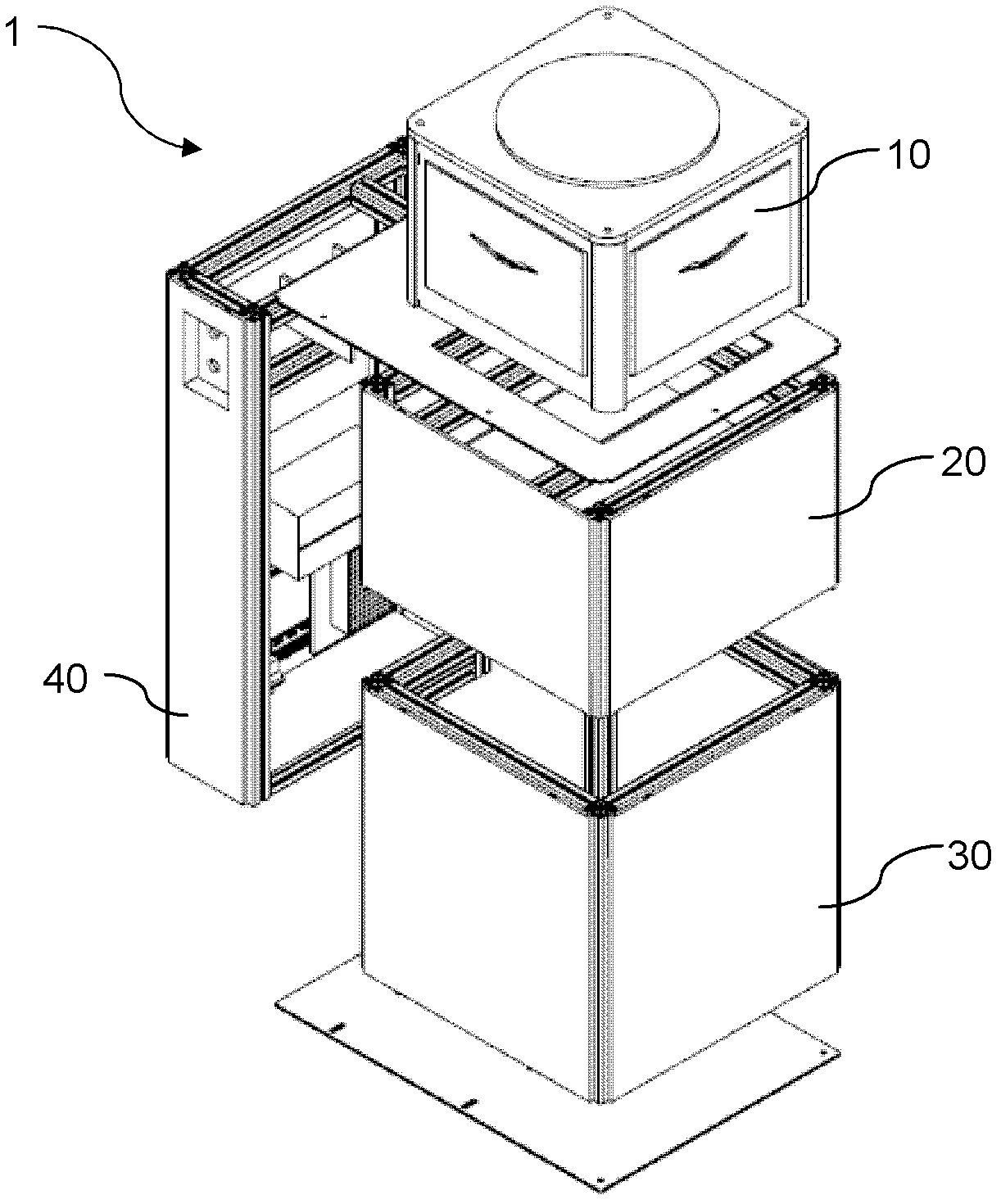
[0044] figure 1 A schematic structural view of the modularized semiconductor processing equipment 1 in the present invention is shown. like figure...


PUM


Abstract

The invention discloses a modularized semiconductor processing device which comprises a semiconductor processing module, a fluid transmission module, a fluid bearing module and a control module. The semiconductor processing module comprises a micro-cavity used for containing and processing a semiconductor wafer. The micro-cavity comprises one or more inlets used for enabling fluid to enter the micro-cavity and one or more outlets used for enabling the fluid to be discharged from the micro-cavity. The fluid transmission module is used for enabling the unused fluid in different kinds to be driven to the micro-cavity through a pipeline and the inlets of the micro-cavity. The control module is used for controlling the semiconductor processing cavity and the fluid transmission module. The semiconductor processing device has the advantages of being small in size, simple in structure, convenient assemble, flexible in assembly, favorable for displacement of components and the like.

Description

【Technical field】 [0001] The invention relates to the field of semiconductor surface treatment, in particular to a modular semiconductor processing equipment for surface treatment of semiconductor wafers. 【Background technique】 [0002] At present, integrated circuits are gradually being applied to many fields, such as computers, communications, industrial control and consumer electronics. The manufacturing of integrated circuits has become a basic industry as important as steel. [0003] Wafers are the carriers used to produce integrated circuits. In actual production, the wafers that need to be prepared have a flat, ultra-clean surface, and the existing methods for preparing ultra-clean wafer surfaces can be divided into two categories: wet processes such as immersion and spray techniques, and processes such as Dry treatment process based on chemical vapor and plasma technology. Among them, the wet processing process is a relatively widely used method in the prior art. ...

Claims


Application Information

Patent Timeline
Patent Type & Authority Applications(China)
IPC IPC(8): H01L21/67H01L21/677
Inventor 温子瑛马彦圣
Owner WUXI HUAYING MICROELECTRONICS TECH CO LTD
Why Eureka
Try Eureka