Semiconductor device and manufacturing method thereof

A technology for semiconductors and devices, applied in the field of semiconductor devices and their manufacturing, can solve the problems of small lower electrode contact area and difficult to meet the driving current, and achieve the effect of reducing the contact area and avoiding the limitation of lithography capability.

Active Publication Date: 2013-07-03
SEMICONDUCTOR MANUFACTURING INTERNATIONAL (BEIJING) CORP
View PDF2 Cites 6 Cited by
  • Summary
  • Abstract
  • Description
  • Claims
  • Application Information

AI Technical Summary

Problems solved by technology

[0006] With the continuous improvement of the integration level of semiconductor devices, the requirement for the low value of the driving current is getting higher and higher, but the driving current of the existing devices is difficult to meet this requirement
This is because, in the existing phase change unit, the upper electrode / phase change material / lower electrode connection method is adopted, and it is difficult to obtain a smaller contact area of ​​the lower electrode by using the existing photolithography and etching process

Method used


Image

  • Semiconductor device and manufacturing method thereof
  • Semiconductor device and manufacturing method thereof
  • Semiconductor device and manufacturing method thereof

Examples


preparation example Construction

[0075] The formation process of the phase change unit and the sidewall electrodes can be the same as the preparation method in the previous embodiment. The method can include:

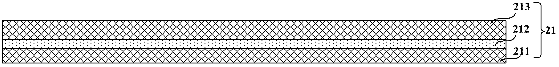
[0076] First, the lower insulating material layer 211, the phase change material layer 212 and the upper insulating material layer 213 are sequentially deposited on the first insulating material layer 251, as Figure 4D shown.

[0077] The material of the two insulating material layers may be insulating oxide. Wherein, the materials of the lower insulating material layer 211 and the upper insulating material layer 213 may be the same or different. The material of the phase-change material layer 212 may be GeSbTe chalcogenide, such as GeSbTe, N-Ge-Sb-Te, As-Sb-Te or In-Sb-Te.

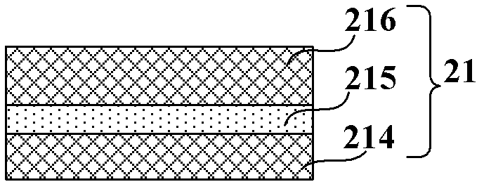
[0078] Then, part of the materials of the above three layers are removed by etching to form the phase change unit 21 . The formed phase change unit 21 includes a lower insulating material layer 214 , an upper insulating mater...


PUM


Abstract

The invention discloses a semiconductor device and a manufacturing method thereof. The semiconductor device comprises a phase change unit and two side wall electrodes, wherein the side wall electrodes are respectively located on two opposite side walls of the phase change unit. The phase change unit comprises three structures, wherein a phase change material layer is clamped between an upper insulation material layer and a lower insulation material layer. The first side wall electrode and the second side wall electrode contact the end face of the phase change material layer. By arranging the side wall electrodes, the connection method of the electrodes and phase change material is changed, the contact area of the electrodes and the phase change material can be reduced by utilizing existing preparation technique, therefore small driving current can be obtained, and the continually-improving demands of semiconductor device integration can be met.

Description

technical field [0001] The invention relates to the semiconductor field, in particular to a semiconductor device and a manufacturing method thereof. Background technique [0002] With the rapid development of the information industry, the requirements for memory are getting higher and higher. Phase-change random access memory (PCRAM) has the advantages of high-efficiency reading, high erasability, non-volatility, small cell area, low power consumption, low cost, multi-level storage, strong shock resistance and radiation resistance. It has become a research hotspot of storage technology at present. [0003] Phase change random access memory utilizes the property that phase change materials have different resistance values ​​in different states to record data. When the phase change material is in a crystalline state, it has a lower electrical resistance, and when the phase change material layer is in an amorphous state, its electrical resistance is higher. Therefore, data c...

Claims


Application Information

Patent Timeline
Patent Type & Authority Applications(China)
IPC IPC(8): H01L45/00H01L27/24G11C11/56
CPCH10B63/20H10N70/8416H10N70/231H10N70/8828H10N70/063H01L29/12
Inventor 徐佳吴关平刘燕任佳栋
Owner SEMICONDUCTOR MANUFACTURING INTERNATIONAL (BEIJING) CORP
Why Eureka
Try Eureka