
Single-cell/single-molecule imaging light/electricity comprehensive tester based on multifunctional probe

A multifunctional, probe technology, applied in the field of cell imaging and analysis, which can solve the problems of quantitative detection of localization, inability to measure small molecules, and inability to establish the correlation between biochemical molecules released by cells and cell membrane surface properties/channel positions, etc. The effect of spatiotemporal resolution

Active Publication Date: 2013-07-10
SOUTHWEST UNIV
View PDF3 Cites 13 Cited by
  • Summary
  • Abstract
  • Description
  • Claims
  • Application Information

AI Technical Summary

Problems solved by technology

Although AFM has provided many conveniences for the research of life sciences, it still has the following shortcomings: (1) It cannot measure the small molecules released by cells or in the solution environment; (2) It cannot measure the changes of biochemical indicators in the internal metabolic process of a single cell ; (3) It is impossible to realize the localization research at the subcellular and molecular level in the cell; (4) After obtaining the cell surface topography, it is impossible to quantitatively detect the optical / electrical signals at the subcellular and molecular level in the cell at the nanometer scale
However, its shortcomings are: (1) the positioning of the micro-operating system is not precise enough, which is still at the micron level; (2) it is impossible to realize cell surface imaging; (3) it is impossible to establish the relationship between the release of biochemical molecules from cells and the properties of the cell membrane surface / channel position Correlation; (4) detection and localization only at the subcellular level

Method used


Image

  • Single-cell/single-molecule imaging light/electricity comprehensive tester based on multifunctional probe
  • Single-cell/single-molecule imaging light/electricity comprehensive tester based on multifunctional probe
  • Single-cell/single-molecule imaging light/electricity comprehensive tester based on multifunctional probe

Examples


Embodiment Construction

[0037] Hereinafter, the preferred embodiments of the present invention will be described in detail with reference to the accompanying drawings; it should be understood that the preferred embodiments are only for illustrating the present invention, not for limiting the protection scope of the present invention.

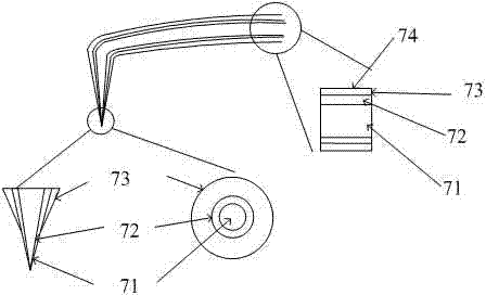
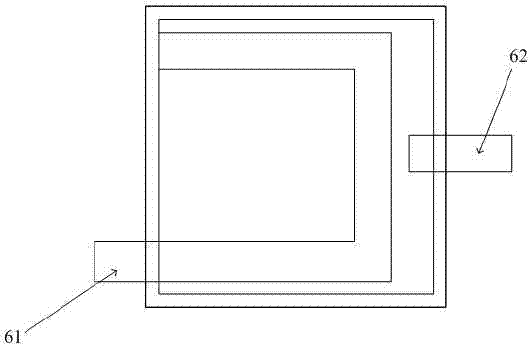
[0038] Figure 1 is a schematic diagram of the nano AFM dual-function probe structure, Figure 2 is a top view of the sample cell structure, Figure 3 is a side view of the sample cell structure, and Figure 4 is a schematic diagram of the structure of the present invention, as shown in the figure: the multifunctional nanometer provided by the present invention The probe is a multifunctional nano probe that can simultaneously realize atomic force microscopy imaging and optical / electrical analysis. When imaging the surface of a single cell or a single biomolecule, the probe can simultaneously emit preset excitation light and electrical signals to the cell and receive the light ...


PUM


Abstract

The invention discloses a single-cell / single-molecule imaging light / electricity comprehensive tester based on a multifunctional probe. The tester comprises the multifunctional nano-probe, a sample pool, an atomic force microscope system, a light source unit, an electricity testing unit, a cell sample locating system and a photon testing unit. The light source unit, the electricity testing unit, the cell sample locating system and the photon testing unit are respectively connected with a data collection and analyzing unit. The multifunctional nano-probe comprises an optical fiber layer, a nano electrode layer and an insulation layer. The nano electrode layer and the insulation layer are wrapped on the outer wall of the optical fiber layer in sequence. The synchronization comprehensive tester comprises a manufacturing method of the nano-probe which can carry out atomic force scanning imaging on single-cells / single-molecules and carry out light / electricity testing at the same time, a manufacturing method of the sample pool and relevant optics, electricity and mechanics testing and analyzing instruments. Temporal-spatial resolution and the range of target objects which can be tested are greatly improved, the tester can be widely used in biology and medicine and be used for fundamental research and disease testing under the level of sub-cells and molecules, and the tester has great development significance on tumor early diagnosis, medicine development and agricultural science.

Description

Technical field [0001] The invention relates to the field of cell imaging and analysis, in particular to an atomic force microscope-based single cell / single molecule real-time imaging and optical / electric analysis synchronous comprehensive tester and a manufacturing method thereof. Background technique [0002] Scanning tunneling microscope (STM) was first invented and used to study the surface morphology and electrical properties of conductors or semiconductors. The principle is to close the sharp nano metal probe tip against the surface of the conductor or semiconductor sample, and apply a potential difference between the two, and realize imaging by detecting the tunnel current. [0003] The subsequent invented Atomic Force Microscope (AFM) makes it possible to image non-conductor materials at the atomic scale. It studies the surface of a substance by detecting the extremely weak interatomic interaction between the surface of the sample to be tested and a miniature force sensitiv...

Claims


Application Information

Patent Timeline
Patent Type & Authority Applications(China)
IPC IPC(8): G01Q60/38G01Q60/24
Inventor 李长明鲁志松郑昕婷
Owner SOUTHWEST UNIV
Learn More