

Manufacturing method for multifunctional projection capacitor touch panel
A technology of touch panel and projected capacitance, which is applied in the direction of electrical digital data processing, input/output process of data processing, instruments, etc. It can solve the problems of weak resistance to external impact, high production cost, and inability to improve the yield rate, etc., to achieve Improvement of external impact ability, improvement of feeling, and reduction of material waste
- Summary
- Abstract
- Description
- Claims
- Application Information
AI Technical Summary
Problems solved by technology
Method used
Image


Examples
Embodiment Construction
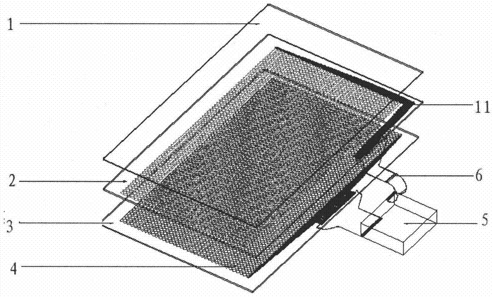
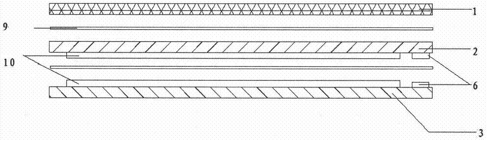
[0019] Such as figure 1 , figure 2 , image 3 , Figure 4 As shown, it includes a structure composed of three layers of substrates, the three layers of substrates are the uppermost cover touch substrate, the middle layer of the drive substrate and the bottom layer of the induction feedback substrate. The respective manufacturing processes of the three-layer substrates are carried out separately and synchronously, and complement each other. After the functional layers on the three-layer substrate are manufactured separately, the driving substrate of the middle layer and the induction feedback substrate of the bottom layer are bonded together with optical glue. Together, and then apply optical glue on the outer surface of the driver substrate, and use the optical glue to attach the cover touch substrate to the outer surface of the driver substrate, so that the three layers of substrates are laminated together. details as follows:
[0020] The manufacturing process of each f...
PUM
 Abstract
Description
Claims
Application Information