Supercharge Your Innovation With Domain-Expert AI Agents!

Manufacturing method of light-emitting diode packaging structure

一种发光二极管、封装结构的技术,应用在电气元件、电固体器件、电路等方向,能够解决影响发光二极管封装结构出光效果、荧光粉分布不均匀等问题

Active Publication Date: 2013-07-10
SUZHOU MEDICAL DEVICE IND DEV CO LTD
View PDF3 Cites 2 Cited by
  • Summary
  • Abstract
  • Description
  • Claims
  • Application Information

AI Technical Summary

Problems solved by technology

Phosphor powder is usually sprayed on the light-emitting surface of the package. However, the randomness of spraying can easily lead to uneven distribution of phosphor powder, or it can be mixed in the packaging material before forming the package body, and it is suspended when the packaging material solidifies. The phosphor powder in the packaging material will be deposited, which will also lead to uneven distribution of the phosphor powder in the cured package body, thus affecting the final light output effect of the LED packaging structure

Method used


Image

  • Manufacturing method of light-emitting diode packaging structure
  • Manufacturing method of light-emitting diode packaging structure
  • Manufacturing method of light-emitting diode packaging structure

Examples


Embodiment Construction

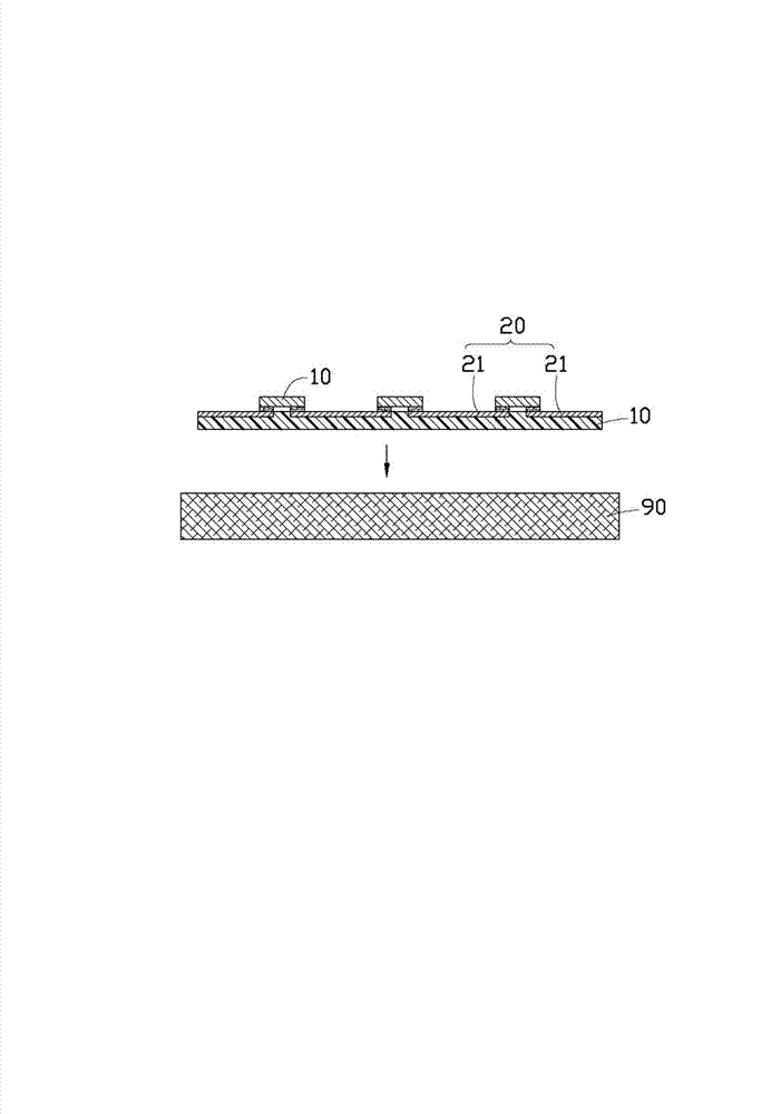
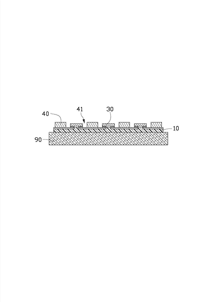
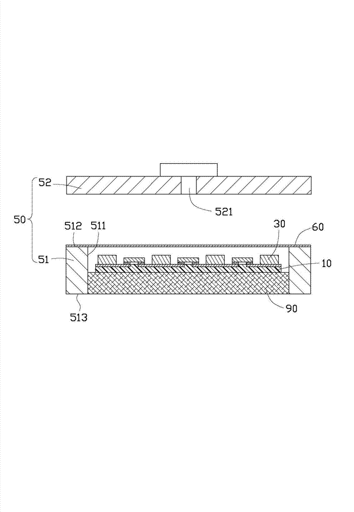
[0019] Such as Figure 9 As shown, the light emitting diode packaging structure 100 provided by the embodiment of the present invention includes a substrate 10, a circuit layer 20 formed on the substrate 10, a light emitting diode chip 30 carried on the substrate 10 and electrically connected to the circuit layer 20, a covering light emitting diode The fluorescent film 60 of the chip 30 and the packaging body 70 encapsulating the LED chip 30 .

[0020] In this embodiment, the light-emitting diode chip 30 is a horizontal structure, which is fixed and electrically connected to the circuit layer 20 of the substrate 10 by a flip-chip method. The LED chip 30 includes a light emitting surface 31 opposite to the substrate 10 , and two electrodes 32 are disposed on the other surface opposite to the light emitting surface 31 . The light emitting surface 31 faces away from the substrate 10 , and the two electrodes 32 face the substrate 10 and are connected to the circuit layer 20 .

...


PUM


Abstract

Provided is a manufacturing method of a light-emitting diode packaging structure. The manufacturing method of the light-emitting diode packaging structure comprises the following steps of providing a substrate and a support plate, and arranging the substrate on the support plate, wherein a circuit layer is formed on the substrate and a plurality of light-emitting diode chips are arranged on the substrate; providing a mold and a luminescence thin membrane, placing the support plate into the mold, and enabling the luminescence thin membrane to seal one end of the mold and to be directly opposite to the light-emitting diode chips, wherein the support plate is arranged at the other end of the mold, and air in the mold is communicated with the external environment through the support plate; removing the air in the mold in a suction mode from the outside of the support plate to enable the luminescence thin membrane to cover the light-emitting diode chips in an attaching mode; removing the mole, and solidifying the luminescence thin membrane; forming a packaging body on the substrate; and cutting the packaging body and the substrate, and removing the support plate to obtain a plurality of light-emitting diode packaging structures.

Description

technical field [0001] The invention relates to a semiconductor manufacturing method, in particular to a manufacturing method of a light emitting diode packaging structure. Background technique [0002] Compared with traditional light sources, light emitting diodes (Light Emitting Diode, LED) have the advantages of light weight, small size, low pollution, long life, etc. As a new type of light source, it has been increasingly used in In various fields, such as street lights, traffic lights, signal lights, spotlights and decorative lights. [0003] Existing LED packaging structures generally include a substrate, electrodes on the substrate, LED chips carried on the substrate and electrically connected to the electrodes, and a package covering the LED chips. In order to improve the luminous characteristics of the light emitting diode chip, phosphor powder is usually arranged in the packaging structure of the light emitting diode. Phosphor powder is usually coated on the ligh...

Claims


Application Information

Patent Timeline
Patent Type & Authority Applications(China)
IPC IPC(8): H01L33/48H01L33/50
CPCH01L24/97H01L33/0095H01L33/486H01L33/50H01L2224/16225H01L2924/12041H01L2924/181H01L2933/0041H01L2924/00H01L33/483H01L33/52
Inventor 陈隆欣曾文良陈滨全
Owner SUZHOU MEDICAL DEVICE IND DEV CO LTD
Features
  • R&D
  • Intellectual Property
  • Life Sciences
  • Materials
  • Tech Scout
  • Unparalleled Data Quality
  • Higher Quality Content
  • 60% Fewer Hallucinations
Learn More