GaAs base multi-layer self-organizing quantum dot structure and preparation method thereof

A technology of self-organized quantum dots and quantum dots, applied in phonon exciters, laser components, electrical components, etc., can solve the problem of weakening the strain accumulation effect, affecting the performance of multi-layer quantum dot device mode gain devices, and electronic wave function overlap The degree of reduction and other issues can be improved to achieve the effect of improving size uniformity, reducing influence, and increasing mode gain

Inactive Publication Date: 2013-07-10
BEIJING UNIV OF POSTS & TELECOMM
View PDF7 Cites 13 Cited by
  • Summary
  • Abstract
  • Description
  • Claims
  • Application Information

AI Technical Summary

Problems solved by technology

When the spacer layer of the adjacent quantum dot layer is thicker (greater than 50nm), the vertical upward propagation of the strain field and the strain accumulation effect will be greatly weakened, and the vertical alignment growth of the quantum dots can be greatly inhibited or even eliminated. The number of dot structure periods can be significantly increased, but the degree of overlap of electronic wave functions between multilayer quantum dots will also be greatly reduced, which ultimately seriously affects the mode gain and device performance of multilayer quantum dot devices.

Method used


Image

  • GaAs base multi-layer self-organizing quantum dot structure and preparation method thereof
  • GaAs base multi-layer self-organizing quantum dot structure and preparation method thereof
  • GaAs base multi-layer self-organizing quantum dot structure and preparation method thereof

Examples


Embodiment Construction

[0039] The specific implementation manners of the present invention will be further described in detail below in conjunction with the accompanying drawings and embodiments. The following examples are used to illustrate the present invention, but are not intended to limit the scope of the present invention.

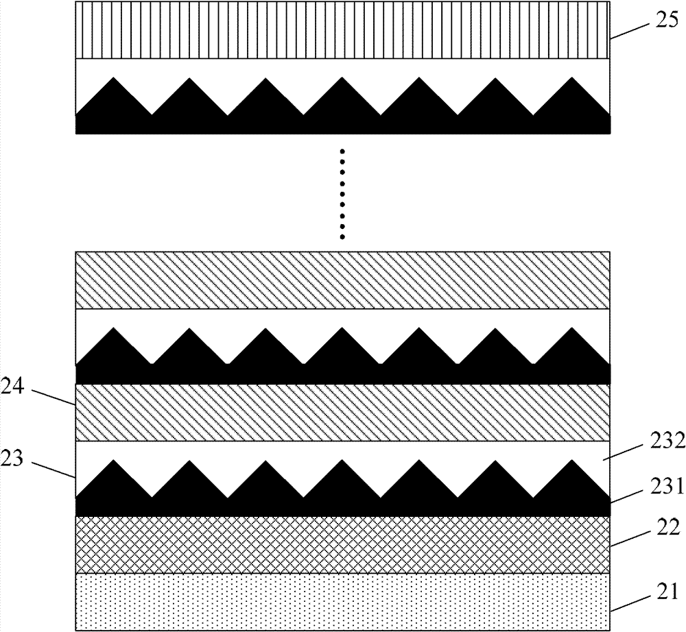
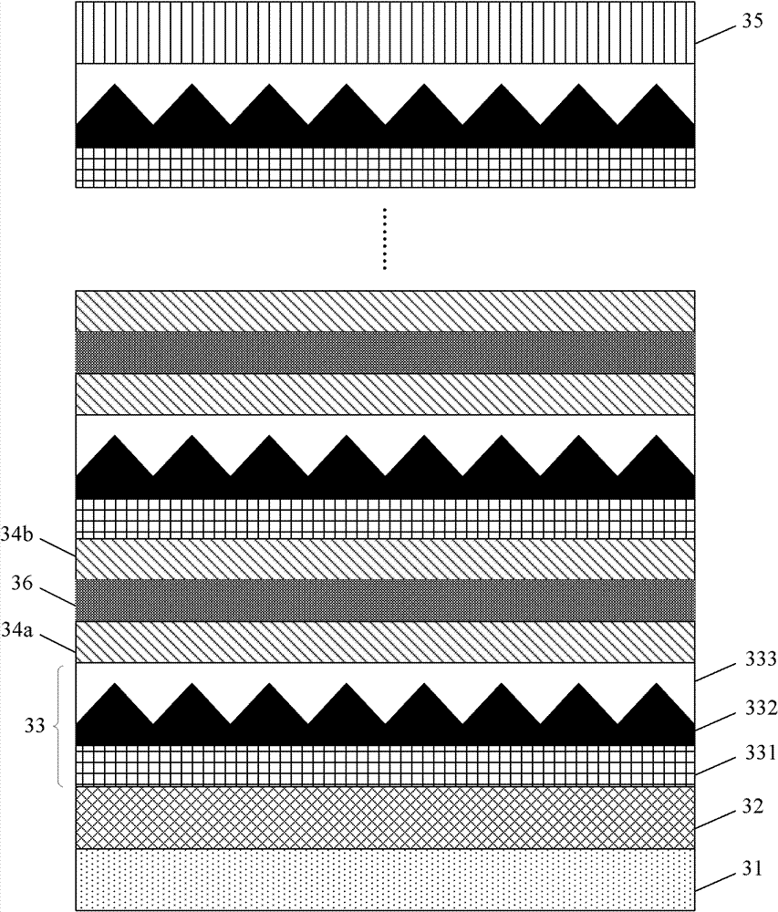
[0040] Such as image 3 As shown, it is the GaAs-based multilayer self-organized quantum dot structure of the embodiment of the present invention, including: a substrate 31, a buffer layer 32 on the substrate 31, an N-layer quantum dot layer 33 on the buffer layer 32, and an N-layer quantum dot layer on the N The cap layer 35 on the layer quantum dot layer 33 is provided with a spacer layer between every two layers of quantum dot layers, and the spacer layer between every adjacent two layers of quantum dot layers 33 is two layers, the first spacer layer 34a and the second spacer layer The second spacer layer 34b is further provided with a strain compensation layer 36 betw...


PUM


Abstract

The invention discloses a GaAs base multi-layer self-organizing quantum dot structure, and relates to the technical field of controllable growth of low-dimension semiconductor quantum dot materials and structures. The structure comprises a substrate, a buffer layer located on the substrate, N quantum dot layers located on the buffer layer and cap layers located on the N quantum dot layers, wherein a spacing layer is arranged between every two quantum dot layers. The structure is characterized in that at least one spacing layer between two adjacent quantum dot layers is double-layer, and a strain compensation layer is arranged between every two spacing layers. The invention further discloses a method for preparing the GaAs base multi-layer self-organizing quantum dot structure. According to the GaAs base multi-layer self-organizing quantum dot structure and the preparation method, strain accumulation among multiple layers of quantum dots is eliminated, accordingly mutual influence among the layers of the quantum dots is effectively reduced, the problem that quantum dots on an upper layer become large due to the strain accumulation is solved, uniformity of the multiple layers of the quantum dots can be improved, and at the same time, periodicity and mode gains of the multi-layer quantum dot structure are improved.

Description

technical field [0001] The invention relates to the technical field of controllable growth of low-dimensional semiconductor quantum dot materials and structures, in particular to a GaAs-based multilayer self-organized quantum dot structure and a preparation method thereof. Background technique [0002] Since the world's first quantum dot laser came out in 1994, GaAs-based InAs and InGaAs quantum dot (Quantum Dot, QD) materials and structures have received great attention. First of all, as a zero-dimensional semiconductor material, quantum dots have many advantages that traditional quantum wells do not have. For example, quantum dots have atomic-like discrete energy levels, making quantum dot devices smaller than traditional quantum well devices. Threshold current density, higher differential gain, higher characteristic temperature, etc. Secondly, the luminescence wavelength of the quantum well structure grown on the GaAs substrate is difficult to reach 1.3 μm, but the InAs ...

Claims


Application Information

Patent Timeline
Patent Type & Authority Applications(China)
IPC IPC(8): H01S5/343
Inventor 王琦贾志刚郭欣任晓敏黄永清
Owner BEIJING UNIV OF POSTS & TELECOMM
Why Eureka
Try Eureka