Method for fabricating thin film transistor

Inactive Publication Date: 2006-03-23
SAMSUNG DISPLAY CO LTD
View PDF4 Cites 12 Cited by
  • Summary
  • Abstract
  • Description
  • Claims
  • Application Information

AI Technical Summary

Benefits of technology

[0010] The present invention, therefore, can help to solve problems associated with conventional devices by providing a method of fabricating a TFT. For example, a metal catalyst layer can be formed using a sputtering target that includes an alloy of a metal catalyst and a metal with a larger atomic weight than the metal catalyst. The metal catalyst and other metal can be present in a predetermi

Problems solved by technology

However, the solid phase crystallization method has a disadvantage that severe deformation of the substrate may occur when the substrate is annealed for a long time at a high temperature, and the excimer laser crystallization method has disadvantages that not only high-cost equipment and high maintenance cost are required but also the surface roughness of the polycrystalline silicon layer is poor.
In order to solve the above-descr

Method used


Image

  • Method for fabricating thin film transistor
  • Method for fabricating thin film transistor
  • Method for fabricating thin film transistor

Examples


Embodiment Construction

[0017] The present invention will now be described in detail with reference to the accompanying drawings in which example embodiments of the invention are shown. The invention may, however, be embodied in different forms and should not be construed as limited to the embodiments shown and described. The dimensions in the drawings are exaggerated for clarity. The same reference numerals are used to denote the same elements throughout the specification.

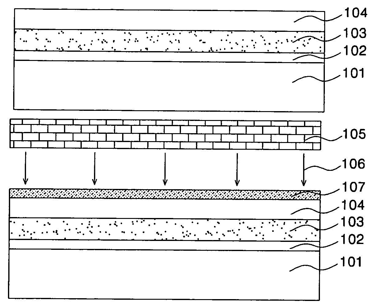
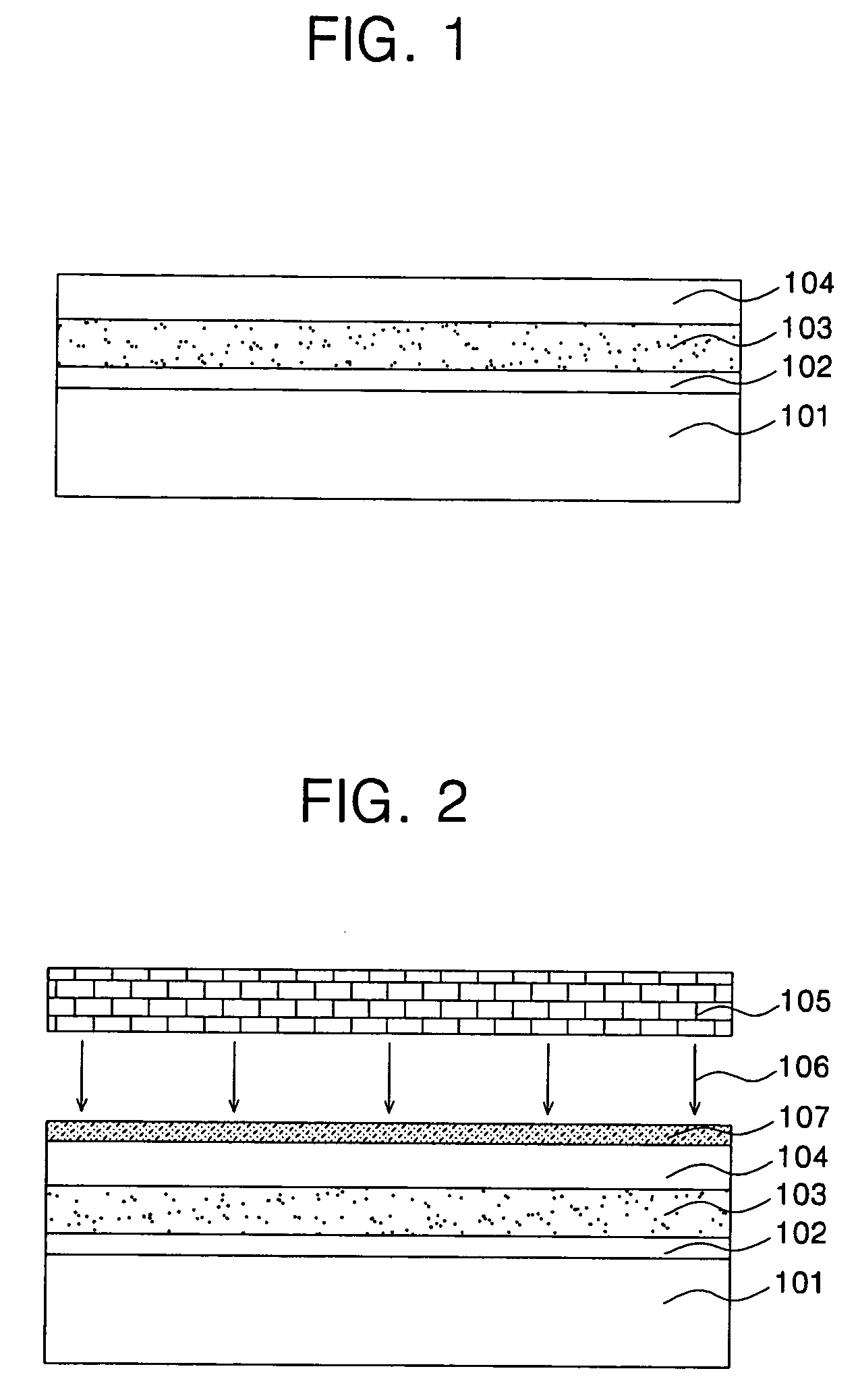
[0018]FIG. 1 is a cross-sectional view of a process of forming a buffer layer, an amorphous silicon layer, and a capping layer on a substrate. As shown in FIG. 1, a single or multi-layer of silicon oxide or silicon nitride can be formed on a transparent substrate 101 such as glass or plastic using chemical vapor deposition (CVD) or physical vapor deposition (PVD). Thus, a buffer layer 102 can be formed. The buffer layer 102 may prevent moisture or impurities generated from the substrate below from diffusing. It can also (or alternativel...


PUM


Abstract

A method of fabricating a thin film transistor can include forming a metal catalyst layer on a substrate on which an amorphous silicon layer and a capping layer are formed. The metal catalyst may be formed using a sputtering target in which a composition ratio of the metal catalyst is controlled in the process of forming the sputtering target. The target may be composed of the metal catalyst and a metal with a larger atomic weight than the metal catalyst. The alloy may be formed with a predetermined composition ratio. The substrate may be annealed to crystallize the amorphous silicon layer to a polycrystalline silicon layer.

Description

CROSS-REFERENCE TO RELATED APPLICATION [0001] This application claims priority to and the benefit of Korean Patent Application No. 2004-76109, filed Sep. 22, 2004, which is incorporated herein by reference in its entirety. BACKGROUND OF THE INVENTION [0002] 1. Field of the Invention [0003] The present invention relates, for example, to a method for fabricating a thin film transistor. More particularly, it relates, for example, to a method for fabricating a thin film transistor that includes forming a metal catalyst layer of a predetermined composition on a substrate. [0004] 2. Description of the Related Art [0005] Generally, thin film transistors (TFTs) used for flat display devices are fabricated as follows. Amorphous silicon is deposited on a transparent substrate such as glass or quartz. The amorphous silicon is then dehydrated and impurity ions for forming a channel are implanted. Subsequently, the amorphous silicon is crystallized to form a semiconductor layer. A gate insulatin...

Claims


Application Information

Patent Timeline
IPC IPC(8): H01L21/84H01L21/00
CPCH01L21/2022H01L29/66757H01L27/1214H01L27/1277H01L21/02422H01L21/02488H01L21/02532H01L21/02672H01L21/02595
Inventor SHIN, HYUN-EOK
Owner SAMSUNG DISPLAY CO LTD
Why Eureka
Try Eureka