A production method for a step stencil

A production method and step technology are applied in the preparation of printing surface, the photoengraving process of pattern surface, printing and other directions to achieve the effects of high positional accuracy, high bonding force and not easy to fall off.

Inactive Publication Date: 2013-07-17
KUN SHAN POWER STENCIL
View PDF6 Cites 3 Cited by
  • Summary
  • Abstract
  • Description
  • Claims
  • Application Information

AI Technical Summary

Problems solved by technology

[0007] Therefore, using the combination of etching and electroforming to prepare metal templates with up steps and down steps on the PCB surface has attracted much attention, but it also has certain challenges.

Method used


Image

  • A production method for a step stencil
  • A production method for a step stencil
  • A production method for a step stencil

Examples


Embodiment Construction

[0082] Embodiments of the present invention are described in detail below, examples of which are shown in the drawings, wherein the same or similar reference numerals designate the same or similar elements or elements having the same or similar functions throughout. The embodiments described below by referring to the figures are exemplary only for explaining the present invention and should not be construed as limiting the present invention.

[0083] The specific technological process of this legal name and the attention problem in technological process among the present invention will be more detailed in the following narration.

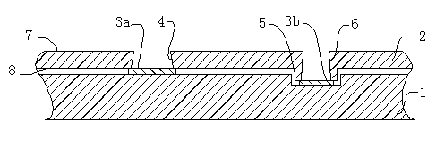
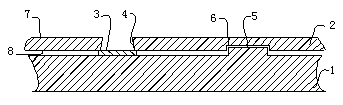
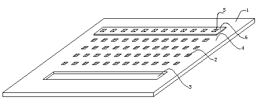
[0084] A method for making a step formwork. Its specific technological process is as follows:

[0085] The first electroforming layer of electroforming: core mold treatment → pretreatment (degreasing, pickling, sandblasting) → film 1 → exposure 1 → single-sided development 1 → electroforming 1;

[0086] Electroformed PCB surface up step: pre-treat...


PUM


Abstract

A production method for a step stencil. Specifically, the production process flow is as follows: electroforming a first electroformed layer: core mold treatment->pre-treatment (degreasing, pickling and sandblasting)->film mounting 1->exposure 1->single sided development 1-> electroforming 1; electroforming up steps on a PCB surface: pretreatment (pickling and sandblasting)->double sided film mounting 2->double sided exposure 2->double sided development 2t->electroforming 2->film stripping->mold stripping; and etching down steps on the PCB surface: double sided film mounting on the electroformed layer->PCB surface exposure->PCB surface development->PCB surface etching ->film stripping->follow-up treatment (degreasing and pickling). By employing the method, the produced electroformed stencil has the PCB surface with up steps and down steps, and the step areas have opening patterns. The method of the invention solves the following technical problems: the pattern openings of the obtained up step area are in high position alignment precision with the openings of the first electroformed layer; the produced entire electroformed stencil has smooth opening hole walls, no undesirable phenomena such as blurs and diffusion coating, good surface quality, no undesirable defects such as pinholes and pittings; the stencil thickness uniformity COV is less than 10%; the stencil surface is in first grade brightness; and the bonding strength of the electroformed layer of the up step area and the first electroformed layer is strong, without the proneness of falling off.

Description

[0001] technical field [0002] The invention relates to a method for making a stepped template, which belongs to the field of material manufacturing and processing, and in particular to a printing mask in the field of SMT with raised steps and recessed steps on the PCB surface, and both the step region and the plane region have opening patterns production process. [0003] Background technique [0004] With the pursuit of miniaturization of electronic products, the perforated plug-in components used before can no longer be reduced; the functions of electronic products are more complete, and the integrated circuits (ICs) used can no longer perforate components, especially large-scale and highly integrated ICs, which have to use surface SMT components, so the stencil printing process has developed rapidly in the electronics manufacturing industry, and SMT printing is a typical example. The procurement of templates is not only the first step in the SMT assembly process, but ...

Claims


Application Information

Patent Timeline
Patent Type & Authority Applications(China)
IPC IPC(8): B41C1/12B41N1/04B41N3/03G03F7/00
Inventor 魏志凌高小平赵录军
Owner KUN SHAN POWER STENCIL
Why Eureka
Try Eureka