A hybrid preparation process for a three-dimensional mask plate
A three-dimensional, preparation process technology, applied in printing plate preparation, printing, assembling printed circuits with electrical components, etc., to achieve the effect of smooth and uniform layout, improved hole wall quality, and improved interface bonding force
- Summary
- Abstract
- Description
- Claims
- Application Information
AI Technical Summary
Problems solved by technology
Method used
Image

Examples
Embodiment 1
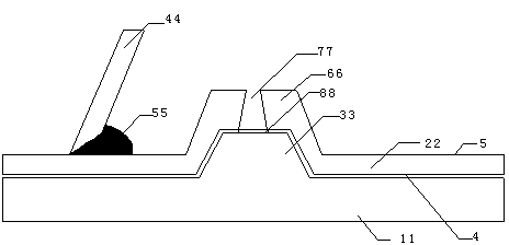
[0112] In an embodiment of the present invention, the preferred process steps in electroforming the first electroforming layer are as follows:
[0113] (1) Mandrel pretreatment: select 1.8mm thick 304 stainless steel plate as the mandrel material, cut the mandrel into a size of 800mm*600mm, and then degrease, pickle and sandblast the mandrel, and the degreasing time 2min, pickling time 1min, sandblasting time 3.5min, sandblasting particle size 1-10μm, sandblasting pressure 2psi;
[0114] (2) Film 1: Apply film to the surface of the mandrel;
[0115] (3) Exposure 1: Expose the pattern opening area and the part other than the alignment hole area, so that the unexposed area can be removed by development, and the exposed part is left as a protective film for the subsequent electroforming step. The exposure amount is 1500mJ, and the exposure time 1200s;
[0116] (4) Single-sided development 1: Clean off the dry film of the developed part except the pattern opening area and the al...
Embodiment 2
[0120] According to the (5) electroforming step in Example 1, preferably, the electroforming process parameters used are as follows:
[0121] Current density (A / m 2 ) 2.3
[0122] Electroforming time 1(min) 150
[0123] Temperature (℃) 50±1
[0124] pH 4-4.5
[0125] Activation time 1 (min) 3
[0126] Electroforming solution composition:
[0127] Nickel sulfamate (g / L) 60
[0128] Nickel chloride heptahydrate (g / L) 14
[0129] Boric acid (g / L) 35
[0130] Brightener (ml / L) 2.1
[0131] Stabilizer (ml / L) 3
[0132] Wetting agent (ml / L) 2
Embodiment 3
[0134] In an embodiment of the present invention, a preferred process step of electroforming the protrusion of the printing surface is as follows:
[0135] (1) Pretreatment: pickling and sandblasting the mask plate prepared in step A, wherein the pickling time is 2 minutes, the sandblasting time is 5 minutes, the sandblasting particle size is 1-10 μm, and the sandblasting pressure is 5 psi;
[0136] (2) Reverse film 2: the printed surface film of the electroformed layer prepared in step A;
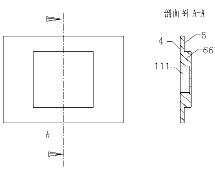
[0137] (3) Alignment: CCD alignment is performed through the alignment hole of the electroforming layer to determine the origin of the coordinates;
[0138] (4) Exposure 2: The exposure area is other than the three-dimensional area (convex area), the exposure amount is 2000mJ, and the exposure time is 2500s;
[0139] (5) Single-sided development 2: Clean and remove the film on the unexposed part, keep the film on the exposed part, and the developing time is 360s;
[0140] (6) Electroform...
PUM
 Abstract
Description
Claims
Application Information