

Packaging module with embedded package and manufacturing method thereof
A technology for encapsulating modules and manufacturing methods, which is applied in semiconductor/solid-state device manufacturing, electric solid-state devices, semiconductor devices, etc., and can solve problems such as electrical failure of the overall encapsulation module, reduction in encapsulation yield, circuit breakage or short circuit in the carrier board, etc.
- Summary
- Abstract
- Description
- Claims
- Application Information
AI Technical Summary
Problems solved by technology
Method used
Image

Examples
Embodiment 1
[0029] refer to Figure 1A to Figure 1H , which is a schematic flow chart of manufacturing the package in this embodiment.
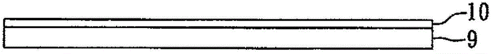
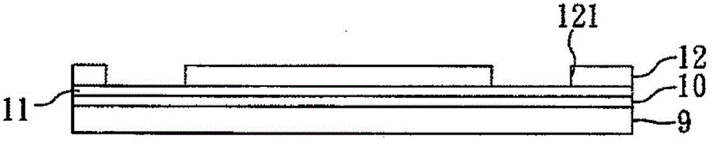
[0030] First, if Figure 1A As shown, a carrier board 9 is provided, and a release film 10 is pasted on the surface of the carrier board 9 . The materials of the release film 10 and the carrier plate 9 are not particularly limited, and materials commonly used in the present invention can be used. Next, if Figure 1B As shown, a conductive layer 11 is pasted on the surface of the release film 10, and a patterned resistance layer 12 is formed on the surface of the conductive layer 11 by photolithography, wherein the resistance layer 12 has a plurality of openings. Hole 121. In this embodiment, a metal copper foil with a thickness of about 18 μm is used as the conductive layer 11 , and the material used for the resistive layer 12 is a photoresist material commonly used in the field.
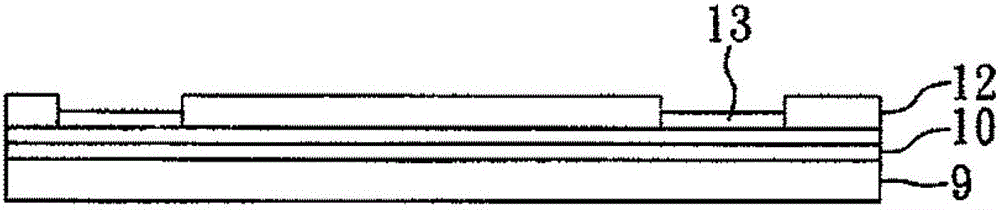
[0031] Such as Figure 1C As shown, using the conductive layer 11 a...
Embodiment 2
[0036] refer to Figure 1A to Figure 1I , which is a schematic flow chart of manufacturing the package in this embodiment.
[0037] The method for manufacturing the package body 1' of the present invention in this embodiment is roughly similar to the above-mentioned embodiment 1, the difference lies in Figure 1F The step is to place the adhesive film 14 on the chip installation area Z first, and then place the first semiconductor chip 15 on the adhesive film 14 with the first passive surface 15b facing the adhesive film 14. chip setting area Z; and, finally as Figure 1I As shown, at the position corresponding to the first electrical connection pad 13 on the first packaging material 17, a conductive via 18 is opened to pass through the first packaging material 17 and connect to the first electrical connection pad 13, wherein, The first packaging material 17 exposes the conductive via 18 on the second surface 1b. The method of forming the conductive via 18 is not particularl...
Embodiment 3
[0039] refer to Figure 2A to Figure 2C , which is a schematic flow chart of manufacturing the packaging module in this embodiment.
[0040] First, if Figure 2A As shown, a packaging substrate 30 and a second semiconductor chip 20 are provided, wherein the packaging substrate 30 has a second electrical connection pad 301, and the second semiconductor chip 20 has a second active surface 20a, a second passive surface surface 20b, and a second electrode pad 201 located on the second active surface 20a. A third adhesive film 21 is pasted on the second passive surface 20b of the second semiconductor chip 20 .
[0041] Next, if Figure 2B As shown, the second semiconductor chip 20 is disposed on the surface of the packaging substrate 30 having the second electrical connection pad 301 through the third adhesive film 21 . In addition, a second adhesive film 22 is used to attach between the second surface 1 b of the package 1 prepared in the first embodiment and the second active ...
PUM
 Abstract
Description
Claims
Application Information