Accurate circuit board element location and detection method based on image feature

A precise positioning, circuit board technology, applied in measurement devices, optical testing flaws/defects, instruments, etc., can solve problems such as difficulty in detecting artificial electronic components, and achieve the effect of realizing industrial production automation, stable matching results, and high detection quality.

Inactive Publication Date: 2013-07-24
TIANJIN UNIV
View PDF3 Cites 25 Cited by
  • Summary
  • Abstract
  • Description
  • Claims
  • Application Information

AI Technical Summary

Problems solved by technology

[0003] In order to overcome the increasingly difficult problem of manual electronic component detection, the present invention provides a method for circuit board positioning and defect detection based on image features

Method used


Image

  • Accurate circuit board element location and detection method based on image feature
  • Accurate circuit board element location and detection method based on image feature
  • Accurate circuit board element location and detection method based on image feature

Examples


Embodiment Construction

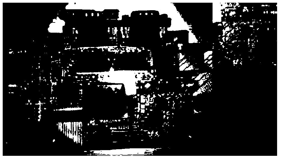
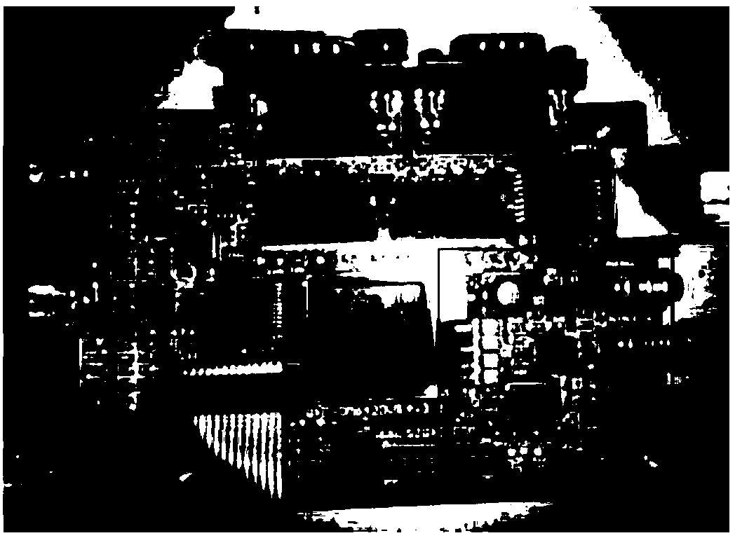
[0017] In the application of circuit board component positioning and detection, the picture of the circuit board to be tested is collected first, and the characteristic point pairs of the collected picture and the standard circuit board component template picture are obtained through the SURF algorithm. In general, SURF-based image matching does not require image preprocessing. In special cases, it is subject to external environment interference (such as underwater), and some preprocessing of the image (image enhancement, filtering, smoothing) is required. etc.). The Accelerated Robust Feature (SURF) algorithm was proposed by Bay et al. in 2006. It is an algorithm with invariance to image perspective, scale, rotation and illumination changes. It is aimed at the SIFT proposed by Lowe et al. Algorithm improvements. Image matching based on SURF algorithm is mainly divided into three steps: feature point extraction, feature point description and feature point matching. Bay et al....


PUM


Abstract

The invention belongs to the technical field of circuit board defect detection, and relates to an accurate circuit board element location and detection method based on image feature. The method comprises the following steps of acquiring a picture of a to-be-detected circuit board, obtaining the acquired image of the to-be-detected circuit board and the feature points of a standard circuit board element template picture through a SURF (Speeded Up Robust Feature) algorithm; setting a rough matching threshold value T, performing feature point rough matching through a nearest neighbor matching method, and then, arranging the feature point pairs from small to large; fitting the ratio of nearest neighbor to next nearest neighbor of each arranged feature point pair through a least square method to obtain a fitted curve; performing accurate matching according to the difference between the fitted curve and the ratio of nearest neighbor to next nearest neighbor; realizing accurate location of the template picture on the acquired image; and detecting the defects of the circuit board through the template picture and the matched subpictures. According to the method, the accurate location of elements can be realized, so that detection on the circuit board elements can be realized.

Description

Technical field [0001] The invention belongs to the technical field of circuit board defect detection and relates to a method for precise positioning and detection of circuit board components. Background technique [0002] With the continuous progress and development of modern science and technology, the functions of electronic products are becoming more and more complex, the performance is improved, the components are getting smaller, and the density is increasing. In the process of circuit board production, there will inevitably be defects such as missing components, offsets, and wrong parts, which lead to manual visual inspection. The circuit board components are difficult and cannot meet the requirements of practical applications. Using image matching technology to detect is of great significance to industrial automation, improving product quality, increasing productivity and saving costs. Image matching is a key technology in digital image processing. How to achieve hi...

Claims


Application Information

Patent Timeline
Patent Type & Authority Applications(China)
IPC IPC(8): G01N21/88G01B11/00
Inventor 肖夏赵玉茹
Owner TIANJIN UNIV
Why Eureka
Try Eureka